ALLPCB


Designing a high-voltage PCB requires careful attention to pad-to-pad spacing to ensure safety and reliability. Proper spacing prevents electrical arcing, maintains insulation, and adheres to industry standards like IPC-2221. In this comprehensive guide, we’ll dive into the essentials of high voltage PCB clearance, creepage distance design, insulation requirements, and arc prevention techniques. Whether you're an engineer working on power electronics or a designer tackling high-voltage applications, this post will equip you with the knowledge to create safe and reliable PCB layouts.
Why Pad-to-Pad Spacing Matters in High-Voltage PCB Design
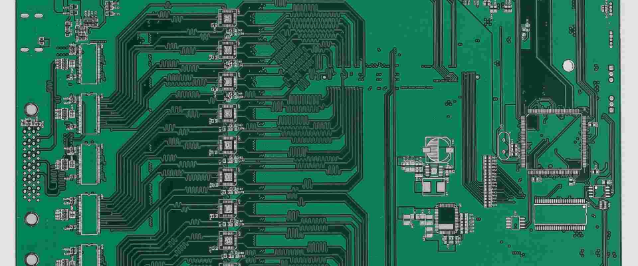
Pad-to-pad spacing is a critical factor in high-voltage PCB design. When voltages exceed a certain threshold—often above 100V—insufficient spacing between conductive pads can lead to electrical breakdown, arcing, or short circuits. These issues not only damage the board but can also pose serious safety risks, including fire hazards or equipment failure.
In high-voltage designs, spacing ensures that the electric field between pads doesn’t exceed the dielectric strength of the surrounding material, whether it’s air or the PCB substrate. By mastering spacing rules, you protect your design from catastrophic failures and extend its operational lifespan. Let’s explore the key concepts and standards that govern this process.
Understanding High Voltage PCB Clearance and Creepage Distance
Two fundamental concepts in high-voltage PCB design are clearance and creepage distance. Both relate to spacing but address different risks.
What Is Clearance?
Clearance refers to the shortest distance through air between two conductive elements, such as pads or traces. It’s crucial for preventing electrical arcing, where a high voltage causes a spark to jump across a gap. For example, at 500V, the clearance distance in air should typically be at least 2.5mm to avoid breakdown, though this varies based on environmental factors like altitude or humidity.
What Is Creepage Distance?
Creepage distance is the shortest path along the surface of the PCB material between two conductive elements. This spacing prevents tracking, a phenomenon where contaminants like dust or moisture create a conductive path over the board’s surface, leading to leakage currents or shorts. Creepage distances are often larger than clearance because surface contamination can lower the insulation resistance. For a 500V application on a standard FR-4 material, a creepage distance of 3.2mm or more might be required depending on the pollution degree.
Both clearance and creepage are influenced by factors like voltage level, material properties, and environmental conditions. Industry standards provide specific guidelines to ensure safety, which we’ll cover next.
IPC-2221 High Voltage Spacing Guidelines
The IPC-2221 standard is a widely accepted guideline for PCB design, including high-voltage applications. It provides detailed requirements for spacing based on voltage levels, ensuring that designs meet safety and reliability criteria. Here’s a breakdown of how IPC-2221 applies to pad-to-pad spacing.
Spacing Based on Voltage Levels
IPC-2221 categorizes spacing requirements by voltage ranges and whether the conductors are on the same layer (internal or external) or between layers. For instance:
- For voltages between 101-150V, the minimum clearance for external conductors is 0.6mm.
- For voltages between 301-500V, this increases to 1.5mm for external conductors and 0.8mm for internal conductors.
- Above 500V, spacing scales further, often requiring 2.5mm or more for external layers.
Creepage distances are also specified and depend on the material’s Comparative Tracking Index (CTI), which measures its resistance to surface tracking. For a material with a CTI of 175-400 (common for FR-4), creepage distances might be 2-3 times the clearance for the same voltage.
Environmental and Material Factors
IPC-2221 also considers environmental conditions like pollution degree (levels of contamination) and overvoltage categories. For example, a PCB in a clean, controlled environment (Pollution Degree 1) requires less creepage than one in a dusty industrial setting (Pollution Degree 3). Designers must account for these variables to meet the standard’s requirements.
By adhering to IPC-2221 high voltage spacing rules, you ensure your design withstands operational stresses and complies with safety regulations. Tools like clearance calculators based on IPC-2221 can simplify this process by providing precise spacing values for your specific voltage and conditions.
Insulation Requirements for High-Voltage PCBs
Insulation is another cornerstone of high-voltage PCB safety. It prevents unintended current flow between conductive elements and protects against breakdowns. Here are the key insulation requirements to consider.
PCB Material Selection
The choice of PCB substrate material impacts insulation performance. Standard FR-4 has a dielectric strength of about 20kV/mm, suitable for moderate high-voltage applications up to 1kV. For higher voltages, materials like polyimide or high-voltage laminates with dielectric strengths of 30kV/mm or more may be necessary. Additionally, the material’s CTI value affects creepage requirements, as discussed earlier.
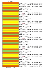
Layer Stackup and Insulation Thickness
In multilayer PCBs, the insulation thickness between layers must withstand the voltage difference. For a 1kV potential between layers, a dielectric thickness of at least 0.05mm is often required, though this increases with voltage. Proper stackup design ensures that internal layers maintain adequate separation to prevent breakdown.
Conformal Coating and Potting
For added insulation, consider applying a conformal coating or potting compound. These protective layers increase the effective creepage distance and shield against environmental factors like moisture or dust. A silicone-based coating, for instance, can boost insulation resistance by a factor of 10, making it ideal for harsh environments.
Meeting insulation requirements ensures your PCB operates safely under high-voltage conditions. Always verify material specs and test insulation performance during prototyping to avoid surprises in production.
Arc Prevention Techniques for High-Voltage PCBs
Arcing is a significant risk in high-voltage designs, where a spark can jump between conductors, causing damage or failure. Implementing arc prevention techniques is essential for safety and reliability.
Increase Spacing Beyond Minimums
While standards like IPC-2221 provide minimum spacing values, adding a safety margin can further reduce arcing risk. For a 1kV application, if the minimum clearance is 2.5mm, increasing it to 3mm provides extra protection against unexpected voltage spikes or environmental changes.
Use Slotting or Barriers
Cutting slots or adding physical barriers between high-voltage pads increases the effective creepage distance. A slot of 1mm width between pads can double the surface path length, significantly reducing the chance of tracking or arcing. Barriers made of insulating materials like plastic can also block potential arc paths.
Optimize Trace Routing
Avoid sharp corners in high-voltage traces, as they concentrate electric fields and increase arcing risk. Use rounded corners with a radius of at least 0.5mm to distribute the field more evenly. Additionally, keep high-voltage traces away from ground planes or low-voltage signals to minimize interference and breakdown risks.
Control Environmental Factors
Arcing is more likely in humid or dusty conditions, as these lower the dielectric strength of air. Design enclosures to protect PCBs from such environments, or use dehumidifiers in critical applications. For instance, maintaining relative humidity below 50% can reduce arcing risk by up to 30% at 1kV.
By applying these arc prevention techniques, you can safeguard your high-voltage PCB against one of the most common failure modes, ensuring long-term reliability.
Practical Tips for Designing High-Voltage PCBs
Beyond spacing and insulation, several practical strategies can enhance the safety and performance of your high-voltage PCB design.
Use Design Software with Rule Checking
Modern PCB design tools often include features to enforce clearance and creepage rules based on standards like IPC-2221. Set up design rule checks (DRC) to flag violations during layout. For example, configure a rule to maintain a 2mm clearance for nets above 500V, and the software will alert you to any issues before fabrication.
Test Under Real-World Conditions
Simulate your design under expected operating conditions, including voltage spikes and temperature extremes. Hi-pot (high-potential) testing can verify insulation strength by applying voltages up to 1.5 times the rated value. A successful test at 1.5kV for a 1kV design confirms robust insulation.
Consider Component Placement
Place high-voltage components away from low-voltage areas to minimize interference and arcing risks. Group similar voltage domains together, and use ground planes as shields between high and low-voltage sections. This approach reduces electromagnetic interference (EMI) and enhances safety.
Document and Review
Thoroughly document your design choices, including spacing calculations and material selections. Conduct peer reviews to catch potential oversights. A second set of eyes can identify a missed creepage path or an undersized clearance that could compromise safety.
These practical steps streamline the design process and help you avoid costly errors in high-voltage PCB projects.
Common Mistakes to Avoid in High-Voltage PCB Design
Even experienced designers can make errors in high-voltage layouts. Here are some pitfalls to watch out for:
- Underestimating Environmental Impact: Failing to account for humidity or pollution can lead to insufficient creepage distances. Always design for the worst-case scenario.
- Ignoring Voltage Transients: Temporary spikes, such as those from switching loads, can exceed nominal voltages. Add a 20-30% buffer to spacing to handle transients.
- Overlooking Material Limits: Using standard FR-4 for voltages above 1kV without verifying dielectric strength can result in breakdown. Check material datasheets carefully.
- Poor Trace Design: Sharp angles or overly thin traces in high-voltage areas increase arcing and heating risks. Maintain smooth, wide traces for current capacity and safety.
Avoiding these mistakes ensures your design meets safety standards and performs reliably over time.
Conclusion: Building Safer High-Voltage PCBs with Proper Spacing
Mastering pad-to-pad spacing is essential for creating safe and reliable high-voltage PCBs. By understanding concepts like high voltage PCB clearance and creepage distance design, adhering to IPC-2221 high voltage spacing guidelines, meeting insulation requirements, and applying arc prevention techniques, you can protect your designs from failure. Thoughtful material selection, strategic layout, and rigorous testing further enhance performance.
At ALLPCB, we’re committed to supporting engineers with the tools and expertise needed for successful high-voltage projects. Whether you’re designing for industrial power systems or cutting-edge electronics, proper spacing and design practices are the foundation of safety and reliability. Use this guide as a roadmap to navigate the complexities of high-voltage PCB design with confidence.