 ALLPCB


In the world of high-power electronics, managing heat in a 12-layer PCB is critical to ensuring performance, reliability, and longevity. As designs become more complex with densely packed components and higher power demands, effective thermal management strategies are essential. This blog dives deep into the best practices for 12-layer PCB thermal management, focusing on techniques like thermal vias, heat sinks, simulations, and conductivity optimization to keep your designs cool under pressure.
Whether you're an engineer working on advanced telecommunications equipment or designing power electronics, understanding how to handle heat in a multi-layer board like a 12-layer PCB can make or break your project. Let’s explore actionable solutions tailored to these challenges, including insights on 12-layer PCB thermal vias, heat sinks, thermal simulation, thermal analysis, and thermal conductivity.
Why Thermal Management Matters for 12-Layer PCBs
A 12-layer PCB is often used in applications requiring high-density interconnects, such as servers, industrial controls, and high-frequency communication systems. With so many layers packed into a compact design, heat dissipation becomes a significant concern. Excessive heat can lead to component failure, reduced performance, and even safety hazards. Effective thermal management ensures that your board operates within safe temperature limits, maintaining reliability and efficiency.
In a 12-layer PCB, heat is generated by power-hungry components like processors, power amplifiers, and voltage regulators. Without proper dissipation, this heat gets trapped between layers, causing thermal stress and degrading materials over time. By implementing robust thermal management strategies, you can prevent hotspots, extend the lifespan of your board, and ensure consistent performance.
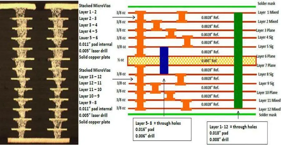
Key Challenges in 12-Layer PCB Thermal Management
Before diving into solutions, it's important to understand the unique challenges of managing heat in a 12-layer PCB:
- High Component Density: With multiple layers, components are packed tightly, leaving little room for natural airflow and increasing the risk of hotspots.
- Limited Space for Cooling: The compact nature of multi-layer boards restricts the use of large cooling solutions like bulky heat sinks.
- Complex Heat Paths: Heat must travel through multiple layers of copper and dielectric materials, each with different thermal conductivities, complicating dissipation.
- Power Demands: High-power applications often push components to generate heat beyond typical thresholds, requiring advanced cooling techniques.
Addressing these challenges requires a multi-faceted approach, combining design techniques and materials optimization. Let’s break down the most effective strategies for 12-layer PCB thermal management.
1. Leveraging 12-Layer PCB Thermal Vias for Heat Dissipation
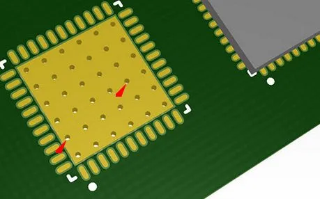
Thermal vias are small, plated-through holes that act as conduits for heat transfer between layers of a PCB. In a 12-layer PCB, where heat can get trapped in inner layers, thermal vias are a critical tool for moving heat to outer layers or a heat sink for dissipation.
How They Work: Thermal vias are typically placed directly under or near high-heat components. They are filled or plated with a conductive material, often copper, to create a low-resistance path for heat to travel. For a 12-layer PCB, thermal vias can connect inner copper planes to outer layers, allowing heat to spread across a larger area or escape into the environment.
Design Tips for 12-Layer PCB Thermal Vias:
- Use a grid or array of vias under heat-generating components to maximize heat transfer. For example, placing 10-15 vias with a diameter of 0.3mm under a high-power IC can reduce junction temperature by up to 10°C.
- Ensure vias are connected to large copper planes on multiple layers to distribute heat evenly.
- Avoid placing thermal vias too close to signal vias to prevent interference with electrical performance.
By strategically integrating 12-layer PCB thermal vias, you can significantly lower operating temperatures and improve reliability in high-power designs.
2. Implementing 12-Layer PCB Heat Sinks for Enhanced Cooling
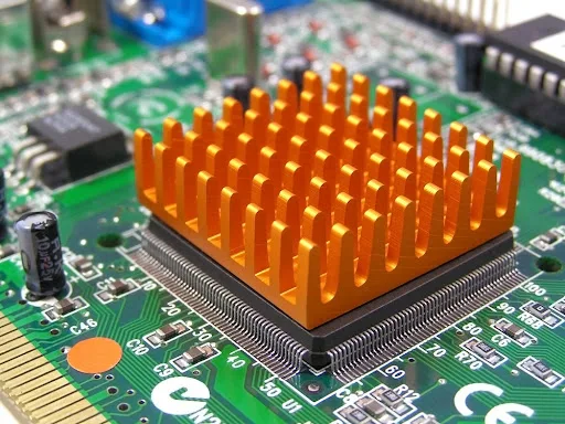
Heat sinks are passive cooling devices that absorb and dissipate heat from components into the surrounding environment. For 12-layer PCBs used in high-power applications, heat sinks are often essential for managing the thermal load of critical components like power transistors or CPUs.
Choosing the Right Heat Sink: The effectiveness of a heat sink depends on its material, size, and design. Aluminum and copper are common materials due to their high thermal conductivity (approximately 205 W/m·K for aluminum and 400 W/m·K for copper). For a 12-layer PCB, compact heat sinks with fins or pin structures are ideal to maximize surface area for heat dissipation without occupying excessive space.
Placement and Attachment:
- Attach heat sinks directly to the top of high-heat components using thermal interface materials (TIMs) like thermal paste or pads to minimize thermal resistance.
- Ensure the heat sink is aligned with thermal vias or copper planes on the PCB to create an efficient heat path.
- In designs with limited vertical space, consider low-profile heat sinks or integrate them with forced airflow for better performance.
Using 12-layer PCB heat sinks in combination with other techniques can keep temperatures within safe limits, even under heavy loads.
3. Utilizing 12-Layer PCB Thermal Simulation for Design Optimization
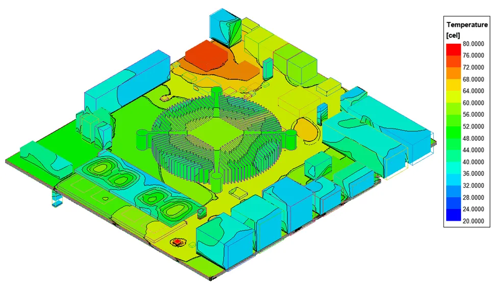
Thermal simulation is a powerful tool for predicting and optimizing heat distribution in a 12-layer PCB before manufacturing. By simulating thermal behavior, engineers can identify potential hotspots, test cooling solutions, and refine their designs without costly physical prototypes.
Benefits of Thermal Simulation:
- Hotspot Detection: Simulation software can model heat generation from components and highlight areas exceeding safe temperature thresholds (e.g., above 85°C for most ICs).
- Design Validation: Test the effectiveness of thermal vias, heat sinks, and copper planes in dissipating heat under various operating conditions.
- Cost Savings: Avoid over-engineering by identifying the minimum number of thermal vias or the optimal heat sink size needed for your design.
How to Perform 12-Layer PCB Thermal Simulation: Use specialized software to input your PCB layout, component power ratings (e.g., a processor dissipating 5W), and material properties. Run simulations under worst-case scenarios, such as maximum ambient temperature or full load, to ensure your design can handle extreme conditions.
Thermal simulation for 12-layer PCBs is a proactive step that saves time and resources while ensuring your board performs reliably in real-world applications.
4. Conducting 12-Layer PCB Thermal Analysis for Performance Insights
While thermal simulation predicts heat behavior during the design phase, thermal analysis involves measuring and evaluating the actual thermal performance of a fabricated 12-layer PCB. This step is crucial for validating your design and identifying areas for improvement.
Key Metrics in Thermal Analysis:
- Junction Temperature: Measure the temperature at the core of critical components. For instance, a junction temperature above 125°C can significantly reduce the lifespan of a semiconductor.
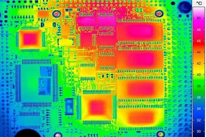
- Thermal Gradients: Analyze temperature differences across the board to detect uneven heat distribution.
- Heat Flow Paths: Assess whether heat is dissipating as intended through vias, copper planes, and heat sinks.
Tools for Analysis: Use infrared (IR) cameras to visualize heat distribution or thermocouples to measure precise temperatures at specific points. Compare these results with simulation data to refine future designs.
Regular 12-layer PCB thermal analysis ensures that your thermal management strategies are effective and helps maintain long-term reliability in high-power applications.
5. Optimizing 12-Layer PCB Thermal Conductivity with Material Selection
Thermal conductivity, measured in W/m·K, determines how well a material transfers heat. In a 12-layer PCB, selecting materials with high thermal conductivity for copper layers, substrates, and thermal interface materials can drastically improve heat dissipation.
Material Considerations:
- Copper Thickness: Use thicker copper layers (e.g., 2 oz or 70 μm) on outer and inner planes to enhance heat spreading. Copper has a thermal conductivity of about 400 W/m·K, making it ideal for thermal management.
- Substrate Materials: Choose substrates with higher thermal conductivity, such as FR-4 with enhanced fillers (around 0.3-0.5 W/m·K) or metal-core PCBs (up to 10 W/m·K) for extreme heat dissipation needs.
- Thermal Interface Materials (TIMs): Use high-conductivity TIMs between components and heat sinks, with values ranging from 1 to 5 W/m·K, to minimize thermal resistance.
Optimizing 12-layer PCB thermal conductivity through smart material choices is a foundational step in managing heat effectively.
Additional Tips for 12-Layer PCB Thermal Management
Beyond the core strategies discussed, here are a few additional tips to further enhance thermal performance:
- Component Placement: Position high-power components away from each other to avoid concentrated heat zones. Place them near board edges for better airflow if possible.
- Forced Air Cooling: In applications where passive cooling isn’t enough, integrate small fans or blowers to improve heat dissipation.
- Copper Pours: Maximize copper coverage on outer layers and connect them to thermal vias to act as heat spreaders.
- Layer Stackup Design: Dedicate specific inner layers as ground or power planes to distribute heat more evenly across the board.
Combining these techniques with the primary strategies ensures a comprehensive approach to thermal management in 12-layer PCBs.
Conclusion: Building Cooler, More Reliable 12-Layer PCBs
Thermal management is a cornerstone of designing high-power 12-layer PCBs. By integrating solutions like 12-layer PCB thermal vias, heat sinks, thermal simulation, thermal analysis, and optimized thermal conductivity, you can prevent overheating, extend component life, and ensure consistent performance. Each strategy plays a unique role in addressing the complex thermal challenges of multi-layer boards, from dissipating heat through vias to predicting issues with simulations.
Start by evaluating your design’s specific heat sources and constraints, then apply the techniques that best suit your needs. With careful planning and the right tools, keeping your 12-layer PCB cool becomes an achievable goal, paving the way for reliable and efficient high-power electronics.
At ALLPCB, we're committed to supporting engineers with the resources and expertise needed to tackle thermal challenges in advanced PCB designs. Explore our services to bring your high-performance projects to life with confidence.





