 ALLPCB


Are you struggling with signal issues on your printed circuit board (PCB) due to impedance mismatches? If you're searching for solutions to PCB impedance mismatch causes, ways of fixing impedance issues in PCBs, or methods for debugging signal reflections on PCBs, you're in the right place. In this comprehensive guide, we'll walk you through the root causes of impedance mismatches, their impact on signal integrity, and practical steps to troubleshoot and resolve these issues effectively.
Impedance mismatches can lead to signal reflections, data errors, and degraded performance in high-speed circuits. Whether you're a seasoned engineer or just starting out, understanding how to identify and fix these problems is crucial for designing reliable PCBs. Let’s dive into the details with actionable advice and real-world insights.
What Is PCB Impedance and Why Does It Matter?
Impedance in a PCB refers to the resistance to the flow of alternating current (AC) signals along a trace. It’s a combination of resistance, capacitance, and inductance, measured in ohms (Ω). In high-speed designs, maintaining consistent impedance is vital to ensure signals travel without distortion or reflection. A typical target impedance for many high-speed digital signals is 50Ω, though this can vary based on the application, such as 75Ω for video signals or 100Ω for differential pairs.
When there’s an impedance mismatch—where the impedance of a trace doesn’t match the source or load—it causes part of the signal to reflect back, leading to interference. This can result in data loss, noise, or complete circuit failure, especially in applications like USB, HDMI, or DDR memory interfaces where signal timing is critical. Understanding and controlling impedance is the foundation of reliable PCB performance.
Common Causes of PCB Impedance Mismatches
Before diving into solutions, let’s explore the key PCB impedance mismatch causes. Identifying the root cause is the first step in troubleshooting.
1. Inconsistent Trace Width and Spacing
Trace width directly affects impedance. For example, a narrower trace increases impedance due to higher resistance and inductance, while a wider trace lowers it. If a trace width varies along its length or doesn’t match the design specifications (e.g., a 10-mil trace for 50Ω impedance), mismatches occur. Similarly, inconsistent spacing between traces in differential pairs can disrupt balanced impedance, often seen in high-speed designs requiring 100Ω differential impedance.
Suggested Reading: How PCB Trace Width Affects Impedance: A Practical Guide
2. Incorrect Stackup Design
The PCB stackup, which defines the arrangement of copper and dielectric layers, plays a huge role in impedance control. If the dielectric thickness or material properties (like dielectric constant, typically around 4.2 for FR-4 material) aren’t accounted for, the impedance can deviate from the target value. For instance, a thinner dielectric layer between a trace and ground plane lowers impedance, causing a mismatch.
3. Poor Termination Techniques
Without proper termination, signals can reflect back at the end of a transmission line. For example, if a 50Ω trace isn’t terminated with a matching 50Ω resistor, the signal bounces back, creating noise. This is common in high-speed designs where termination resistors are omitted or incorrectly valued.
4. Vias and Connectors
Vias, used to connect traces between layers, and connectors can introduce impedance discontinuities. A via might add inductance, altering the impedance locally. For instance, in a 3 GHz signal, even a small via can cause a noticeable reflection if not designed with a proper return path.
5. Manufacturing Variations
During fabrication, variations in trace etching, dielectric thickness, or copper weight can lead to impedance deviations. If a design targets 50Ω but the manufactured trace measures 55Ω due to over-etching, reflections are inevitable. Tight tolerances are essential for high-speed boards to avoid such issues.
Effects of Impedance Mismatches on Signal Integrity
Impedance mismatches don’t just cause theoretical problems—they have real, measurable impacts on your PCB’s performance. Here are the main effects to watch for when debugging signal reflections on PCBs.
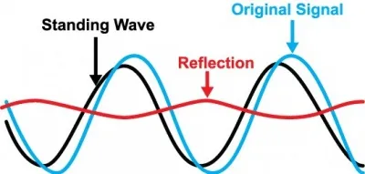
Signal Reflections
When a signal encounters a mismatch, part of it reflects back toward the source. This reflected signal can interfere with the original, causing ringing—oscillations that distort the waveform. For a 2.5 GHz signal, even a small reflection can shift timing enough to cause bit errors.
Crosstalk and Noise
Reflections can couple with nearby traces, inducing crosstalk. This unwanted noise can corrupt data, especially in densely packed boards with traces spaced less than 10 mils apart.
Data Errors and Signal Loss
In high-speed digital systems, reflections can cause voltage levels to fluctuate outside acceptable thresholds. For example, in a DDR3 memory interface operating at 1.5V, a reflection might push the signal below the 0.75V logic threshold, resulting in a misread bit.
Electromagnetic Interference (EMI)
Reflected signals can radiate energy, leading to EMI that interferes with other components or fails regulatory tests. This is a common issue in RF designs where mismatched impedance disrupts signal containment.
Practical Steps for Fixing Impedance Issues in PCBs
Now that we’ve covered the causes and effects, let’s focus on fixing impedance issues in PCBs. These actionable steps will help you troubleshoot and resolve mismatches effectively.
Step 1: Use Impedance Calculators for Design Validation
Before manufacturing, calculate the required trace width and spacing for your target impedance. Online tools or PCB design software can estimate impedance based on stackup, dielectric constant (e.g., 4.2 for FR-4), and trace dimensions. For a 50Ω single-ended trace on a standard 1.6mm board, you might need a trace width of about 10 mils. Validate these calculations early to avoid redesigns.
Step 2: Design a Proper Stackup
Work with your fabrication team to define a stackup that supports your impedance goals. Specify dielectric thickness and material properties clearly. For high-speed signals, ensure a continuous ground plane beneath traces to provide a stable return path, minimizing impedance variations.
Step 3: Implement Termination Strategies
Add termination resistors at the end of transmission lines to match the trace impedance. For a 50Ω line, use a 50Ω resistor to absorb the signal and prevent reflections. Series termination near the source or parallel termination at the load are common techniques, depending on the circuit requirements.
Step 4: Minimize Discontinuities
Reduce the impact of vias by using back-drilling for high-speed signals to remove unused via stubs, which can act as antennas and cause reflections. When routing through connectors, choose ones rated for your signal frequency and impedance, ensuring minimal disruption.
Step 5: Test and Measure Impedance Post-Fabrication
After manufacturing, use a Time Domain Reflectometer (TDR) to measure the actual impedance of traces. A TDR can pinpoint mismatches by showing where reflections occur along a trace. If a section measures 60Ω instead of the target 50Ω, you can trace the issue back to design or fabrication errors.
Debugging Signal Reflections on PCBs: Tools and Techniques
When it comes to debugging signal reflections on PCBs, having the right tools and methods is essential. Here’s how to approach it systematically.
1. Oscilloscope Analysis
Use a high-bandwidth oscilloscope (at least 1 GHz for modern high-speed designs) to observe signal waveforms. Look for ringing or overshoot, which indicate reflections. For example, a clean square wave at 500 MHz should have sharp edges; if edges are distorted, suspect an impedance issue.
2. TDR Measurements
As mentioned earlier, a TDR is invaluable for locating mismatches. It sends a pulse down the trace and measures reflections, providing a map of impedance changes. This is especially useful for identifying issues at vias or connectors.
3. Simulation Software
Before building a prototype, use simulation tools to model signal behavior. Software can predict reflections based on your layout and stackup, allowing you to adjust trace widths or termination before fabrication. This can save significant time and cost.
4. Iterative Testing and Layout Adjustments
If reflections persist, revise the layout. Adjust trace widths, add termination, or reroute signals to avoid discontinuities. Test each iteration with a TDR or oscilloscope to confirm improvements. For instance, widening a trace from 8 mils to 10 mils might bring impedance closer to the target 50Ω.
Best Practices for Preventing Impedance Mismatches
Prevention is always better than troubleshooting. Follow these best practices to minimize impedance issues from the start.
- Collaborate with Fabricators: Share your impedance requirements with your manufacturing partner early. Request controlled impedance traces if needed, which often come with a small additional cost but ensure accuracy within ±10% of the target value.
- Maintain Consistent Routing: Keep trace widths and spacing uniform, especially for differential pairs. Avoid sharp bends, using 45-degree angles or curves to maintain impedance.
- Use Ground Planes: Place a solid ground plane under high-speed traces to stabilize impedance and provide a return path for signals.
- Document Specifications: Clearly define impedance targets, stackup details, and termination needs in your design files to avoid miscommunication during production.

Conclusion: Mastering Impedance Control for Reliable PCBs
Troubleshooting PCB impedance mismatches doesn’t have to be a daunting task. By understanding the PCB impedance mismatch causes, applying strategies for fixing impedance issues in PCBs, and using the right tools for debugging signal reflections on PCBs, you can achieve reliable signal integrity in your designs. Start with proper planning—use calculators, design a solid stackup, and implement termination. Then, test rigorously with tools like TDRs and oscilloscopes to catch issues early.
High-speed electronics demand precision, and impedance control is at the heart of that. With the practical steps and best practices outlined in this guide, you’re equipped to tackle mismatches head-on, ensuring your circuits perform as intended. Keep refining your approach, and your PCBs will deliver consistent, error-free operation even at the highest speeds.


