 ALLPCB


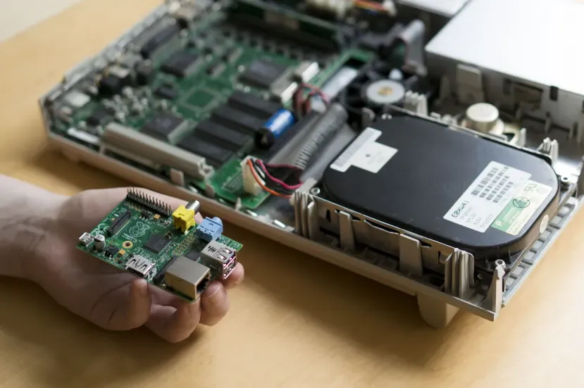
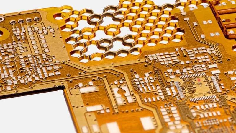
The electronics industry is in a constant race to deliver smaller, more powerful, and feature-rich devices. From smartphones to medical implants, the demand for compact, high-performance electronics has driven the trend of miniaturization in printed circuit board (PCB) design and manufacturing. This shift isn't just about shrinking physical dimensions—it's about redefining how we design, assemble, and optimize PCBs to meet the needs of modern applications. At ALLPCB, we've witnessed firsthand how miniaturization is transforming the industry, presenting both exciting opportunities and complex challenges for engineers.
In this blog, we'll explore the profound impact of miniaturization on PCB design and manufacturing. We'll dive into the technical advancements enabling smaller PCBs, the challenges engineers face, and the strategies to overcome them. Whether you're designing wearables, IoT devices, or automotive systems, understanding these dynamics is critical to staying competitive in today's fast-evolving market.
Why Miniaturization Matters in PCB Design
Miniaturization is the process of designing and manufacturing PCBs with smaller components, reduced physical dimensions, and higher component density. This trend is driven by several key factors:
- Consumer Demand for Portability: Devices like smartwatches, earbuds, and foldable smartphones require compact PCBs to fit into sleek, lightweight form factors. For example, modern smartphones pack over 1,000 components into a PCB area smaller than 100 cm².
- Enhanced Functionality: Smaller PCBs allow more components to be integrated into the same footprint, enabling advanced features like 5G connectivity or AI processing in compact devices.
- Energy Efficiency: Miniaturized components often consume less power, extending battery life in portable devices—a critical factor for IoT sensors and wearables.
- Industry Applications: Industries like medical, aerospace, and automotive rely on miniaturized PCBs for space-constrained applications, such as pacemakers or advanced driver-assistance systems (ADAS).
Key Technologies Driving PCB Miniaturization
Miniaturization is made possible by a combination of advanced design techniques, innovative materials, and cutting-edge manufacturing processes. Below, we explore the most significant technologies enabling this trend.
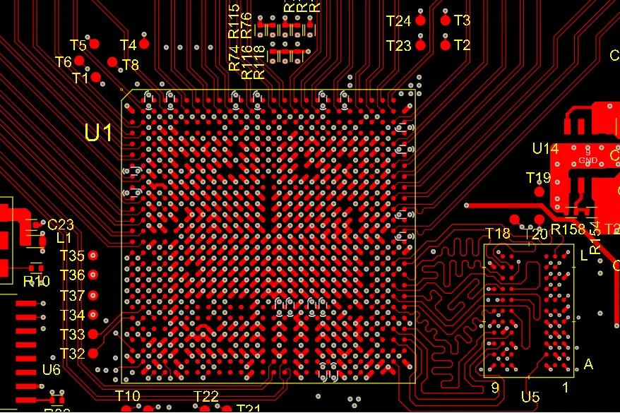
High-Density Interconnect (HDI) PCBs
HDI PCBs are at the forefront of miniaturization, offering higher wiring density per unit area compared to traditional PCBs. They achieve this through:
- Microvias: Laser-drilled vias as small as 50–100 µm allow for denser routing and reduced layer counts. For instance, a 6-layer HDI PCB can achieve the same functionality as a 10-layer standard PCB.
- Fine-Line Traces: Trace widths as narrow as 25 µm (1 mil) enable tighter signal routing, critical for high-speed applications like 5G devices operating at frequencies above 6 GHz.
- Blind and Buried Vias: These vias connect specific layers without penetrating the entire board, saving space and improving signal integrity by reducing parasitic capacitance.
HDI technology is essential for applications like smartphones, where PCB space is at a premium, and signal speeds often exceed 10 Gbps.
Surface Mount Technology (SMT)
SMT has revolutionized PCB assembly by allowing components to be mounted directly onto the board's surface, eliminating the need for through-hole drilling. Key benefits include:
- Smaller Components: SMT supports ultra-small components like 0201 (0.6 mm x 0.3 mm) and 01005 (0.4 mm x 0.2 mm) packages, enabling higher component density.
- Improved Signal Integrity: Shorter trace lengths reduce signal loss and electromagnetic interference (EMI), critical for high-frequency circuits.
- Automation Efficiency: SMT enables automated pick-and-place machines, achieving placement accuracy within ±10 µm, which is vital for densely packed boards.
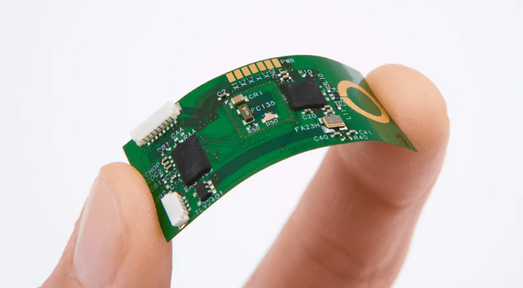
Rigid-Flex and Flexible PCBs
Rigid-flex and flexible PCBs are game-changers for applications requiring non-traditional shapes or dynamic movement, such as wearables or foldable devices. These boards combine rigid sections for component mounting with flexible sections for bending or folding, reducing overall size and weight. For example, a rigid-flex PCB in a medical implant can reduce the device's footprint by up to 50% compared to a rigid PCB.
Advanced Materials
The choice of materials plays a critical role in miniaturization. Key advancements include:
- Low-Dk/Df Laminates: Materials like Rogers RO4000 series, with a dielectric constant (Dk) as low as 3.3, minimize signal loss in high-frequency applications, allowing for tighter trace spacing.
- Thin Substrates: Substrates as thin as 0.1 mm enable multi-layer stacking in compact designs, critical for IoT sensors.
- Conductive Inks: Used in printed electronics, conductive inks allow circuits to be printed on flexible substrates like polyimide, enabling lightweight, bendable PCBs.
Challenges of Miniaturization in PCB Design
While miniaturization unlocks new possibilities, it also introduces significant challenges that engineers must address to ensure performance and reliability.
Signal Integrity and EMI
As components are packed closer together, maintaining signal integrity becomes more difficult. Key issues include:
- Crosstalk: With trace spacing as low as 50 µm, crosstalk can degrade signal quality, especially in high-speed designs operating at 10–20 Gbps.
- Impedance Control: Achieving consistent impedance (e.g., 50 Ω for RF signals) requires precise trace width and spacing, often within ±5% tolerance.
- EMI: Dense component layouts increase the risk of EMI, which can interfere with nearby circuits or violate regulatory standards like FCC Part 15.
Solution: Engineers can use differential signaling, ground planes, and shielding techniques (e.g., metal cans or conductive tape) to mitigate EMI and crosstalk. Simulation tools like Altium Designer can model impedance and signal integrity before fabrication.
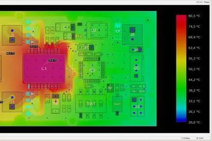
Thermal Management
Miniaturized PCBs generate significant heat in a confined space, especially in high-power applications like automotive ECUs. For example, a densely packed PCB with a power density of 10 W/cm² can exceed safe operating temperatures (typically 85–125°C) without proper cooling.
Solution: Incorporate thermal vias, heat sinks, or high-thermal-conductivity materials (e.g., aluminum-backed PCBs) to dissipate heat. Computational fluid dynamics (CFD) simulations can optimize thermal performance during design.
Manufacturing Complexity
Miniaturization pushes the limits of manufacturing precision, increasing the risk of defects:
- Component Placement: Placing 01005 components requires placement accuracy within ±5 µm, demanding advanced pick-and-place machines.
- Solder Paste Application: Ultra-fine pitch components (e.g., 0.3 mm pitch BGAs) require precise solder paste stencils, often with aperture sizes as small as 100 µm.
- Rework Challenges: Dense layouts leave little room for rework, and overheating during soldering can damage adjacent components.
Solution: Partner with manufacturers equipped with advanced equipment, such as laser direct imaging (LDI) for precise trace patterning and X-ray inspection for solder joint quality.
Design Strategies for Successful Miniaturization
To overcome these challenges, engineers can adopt the following strategies:
- Optimize Component Selection: Choose compact packages like chip-scale packages (CSPs) or wafer-level chip-scale packages (WLCSPs) to reduce footprint. For example, a WLCSP can shrink an IC's size by 30–50% compared to a traditional QFN package.
- Leverage Multi-Layer Designs: Use 8–12 layer HDI PCBs to route complex circuits in a smaller area, balancing layer count with cost.
- Minimize Via Usage: Opt for microvias and staggered via designs to save space and reduce signal path lengths.
- Perform Pre-Layout Simulations: Tools like Cadence Allegro or Mentor Graphics HyperLynx can simulate signal integrity, EMI, and thermal performance, reducing costly design iterations.
- Collaborate Early with Manufacturers: Engage with your PCB manufacturer during the design phase to ensure manufacturability, especially for tight tolerances like 25 µm trace widths.
The Role of ALLPCB in Supporting Miniaturization
At ALLPCB, we empower engineers to tackle the challenges of miniaturization with our advanced manufacturing capabilities and streamlined services. Our quick-turn prototyping allows you to test and refine miniaturized designs in as little as 24 hours, ensuring rapid iteration. We leverage state-of-the-art equipment, such as laser drilling for microvias and automated optical inspection (AOI) for precision assembly, to meet the demands of HDI and rigid-flex PCBs. Our global logistics network ensures fast delivery, while our design for manufacturability (DFM) feedback helps optimize your designs for cost and reliability. Whether you're developing IoT sensors or medical devices, ALLPCB is your partner in bringing compact, high-performance PCBs to life.
Future Trends in PCB Miniaturization
The push for miniaturization shows no signs of slowing down. Emerging trends include:
- 3D PCB Printing: Additive manufacturing techniques, like inkjet printing with conductive inks, enable 3D circuit structures, further reducing size.
- Embedded Components: Embedding passives like resistors and capacitors within PCB layers can reduce surface area by up to 20%.
- Nanotechnology: Advances in nanomaterials, such as graphene-based conductors, promise even smaller, more efficient PCBs with conductivities up to 100 times higher than copper.
- AI-Driven Design: AI tools are optimizing PCB layouts for density and performance, reducing design time by up to 30%.
Conclusion
Miniaturization is reshaping the PCB industry, enabling smaller, more powerful, and energy-efficient devices that drive innovation across industries. However, it demands a careful balance of advanced design techniques, precise manufacturing, and robust testing to overcome challenges like signal integrity, thermal management, and assembly complexity. By leveraging technologies like HDI, SMT, and rigid-flex PCBs, and adopting strategic design practices, engineers can unlock the full potential of miniaturized electronics.
At ALLPCB, we're committed to supporting this evolution with cutting-edge manufacturing and prototyping solutions. As the demand for compact, high-performance devices grows, we invite engineers to partner with us to turn their innovative designs into reality.


