Creating an efficient and reliable printed circuit board (PCB) layout starts with smart component placement. Whether you're focusing on thermal management, high-density designs, or leveraging autorouting tools, the right strategies and PCB component placement software can make all the difference. In this comprehensive guide, we’ll dive into proven techniques for optimizing your PCB layout, including tips for manual placement, thermal considerations, and the best use of design software to streamline the process.
At ALLPCB, we understand the challenges of PCB design and are here to help you achieve high-performance boards with actionable advice and insights. Let’s explore how to master component placement for better functionality, reliability, and manufacturability.
Why Component Placement Matters in PCB Design
Component placement is the foundation of a successful PCB layout. Poor placement can lead to issues like signal interference, excessive heat buildup, or manufacturing difficulties. On the other hand, strategic placement ensures smooth signal flow, effective thermal management, and easier assembly. By using modern PCB component placement software, designers can visualize and refine layouts to avoid common pitfalls.
For instance, placing high-power components too close together without proper spacing can result in thermal hotspots, potentially causing a temperature rise of 20-30°C above safe limits. Similarly, incorrect placement of high-speed signal components can introduce noise, increasing signal delay by as much as 500 picoseconds in critical paths. These numbers highlight why a thoughtful approach, supported by design tools, is essential.
Key Factors in Component Placement for Optimal PCB Layout
Before diving into specific strategies, let’s cover the core factors that influence component placement. These principles guide both manual efforts and software-driven designs, ensuring your PCB performs as intended.
- Signal Integrity: Place components to minimize signal path lengths, especially for high-speed signals. Shorter traces reduce impedance mismatches, often keeping values below 50 ohms for critical lines.
- Thermal Management: Distribute heat-generating components evenly to prevent localized overheating. Consider spacing and heat sinks to maintain temperatures below 85°C for most ICs.
- Power Distribution: Position power components close to their loads to reduce voltage drops, ideally keeping drops below 5% of the supply voltage (e.g., 0.25V for a 5V system).
- Manufacturability: Ensure components are placed with enough clearance for assembly tools, adhering to design-for-manufacturing (DFM) guidelines like 0.5mm spacing between small components.
With these factors in mind, let’s explore specific strategies to optimize your layout using design software and manual techniques.
Using PCB Component Placement Software for Efficient Design
Modern PCB component placement software offers powerful tools to simplify and enhance the design process. These platforms provide features like automated placement suggestions, real-time error checking, and simulation capabilities to test layouts before production.
One major advantage of using such software is the ability to handle complex designs with hundreds of components. For example, in high-density layouts, the software can suggest placements that minimize trace lengths, often reducing total routing distance by 10-15% compared to manual efforts. Additionally, built-in design rule checks (DRC) ensure that spacing and clearance rules are followed, reducing the risk of manufacturing errors by up to 30%.
Many tools also integrate thermal analysis modules. These allow you to simulate heat dissipation across the board, identifying areas where temperatures might exceed safe limits (e.g., above 100°C for certain components). By adjusting placement based on these simulations, you can achieve better thermal management without costly redesigns.
Thermal Management Component Placement: Keeping Your PCB Cool
Effective thermal management component placement is critical, especially for boards with high-power components like processors or power regulators. Overheating can degrade performance or damage components, so strategic placement is key to dissipating heat efficiently.
Start by identifying heat-generating components and placing them away from sensitive parts like sensors or low-power ICs. Aim for a spacing of at least 5-10mm between high-heat components to allow airflow or heat sink integration. If possible, position these components near the board’s edges, where heat can escape more easily.
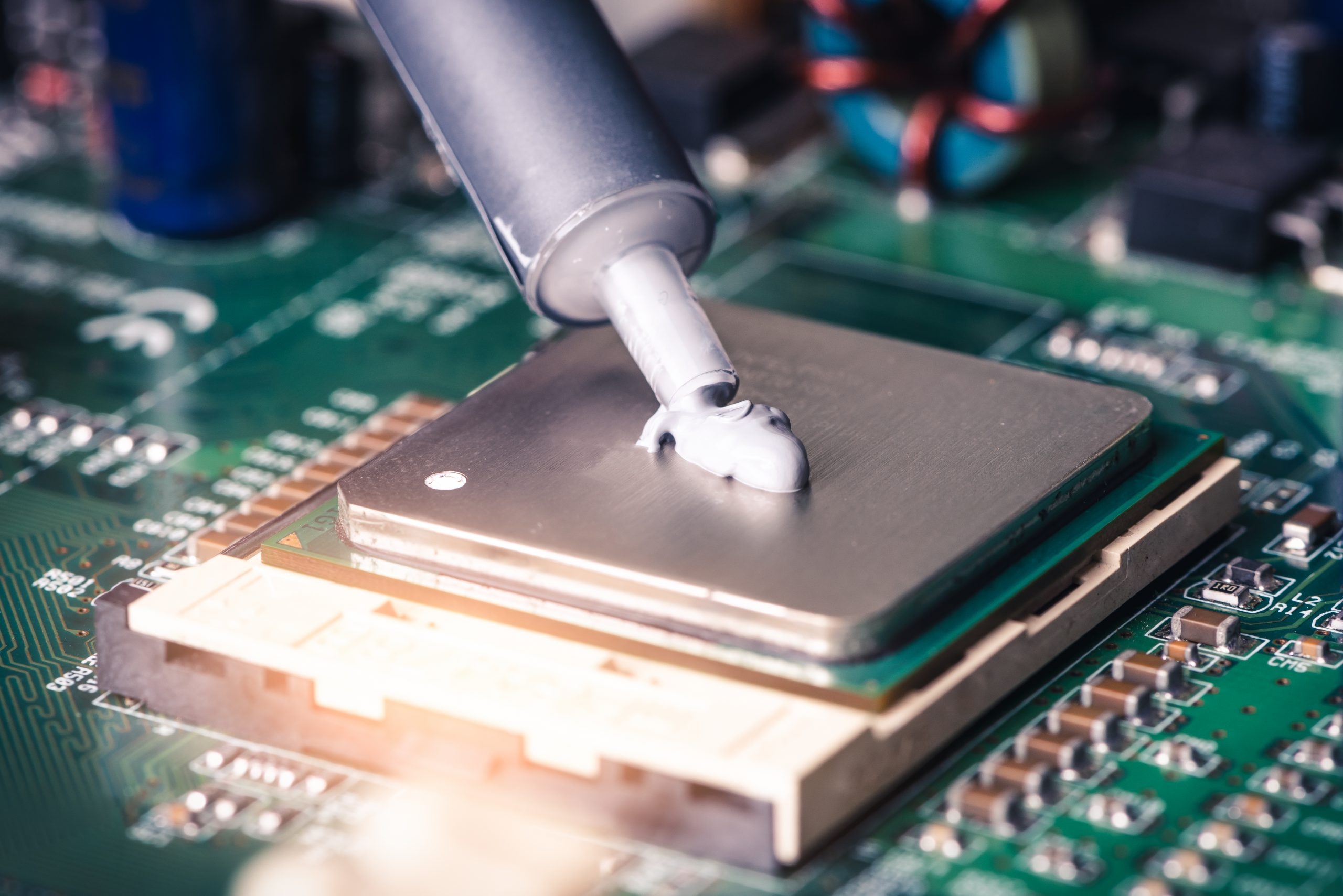
Another tip is to use copper pours or thermal vias under heat-generating components. For instance, a copper area of 2 square inches can reduce component temperature by 10-15°C by acting as a heat spreader. Design software often includes tools to calculate the optimal size and placement of these features, ensuring temperatures stay within safe ranges (e.g., below 85°C for most standard components).
Finally, consider the board’s orientation during operation. If the PCB will be mounted vertically, place hotter components at the top to leverage natural convection, as hot air rises. This simple adjustment can lower peak temperatures by 5-8°C in some designs.
High-Density Component Placement: Maximizing Space Without Sacrificing Performance
In today’s compact electronics, high-density component placement is often necessary to fit more functionality into smaller spaces. However, cramming components together can lead to signal crosstalk, thermal issues, and assembly challenges. Here’s how to manage it effectively.
First, prioritize critical components like microcontrollers or high-speed transceivers by placing them centrally or in areas with minimal interference. Use PCB component placement software to group related components (e.g., decoupling capacitors near ICs), ensuring trace lengths remain short—ideally under 10mm for high-speed signals to keep impedance below 50 ohms.
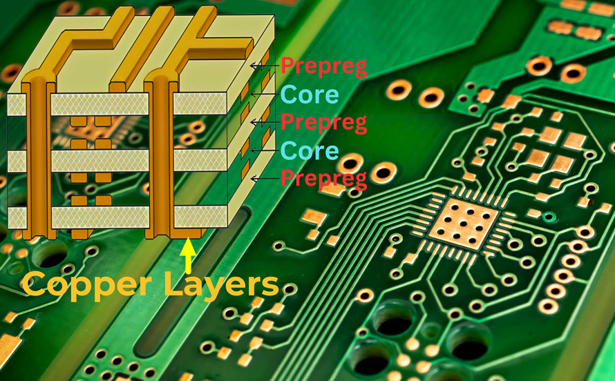
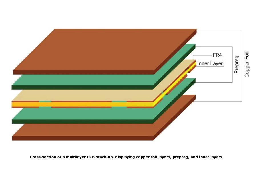
Next, layer components strategically if using a multi-layer board. For example, place power and ground planes on inner layers to shield sensitive signals, reducing electromagnetic interference (EMI) by up to 20 dB. Software tools can help visualize these layers and optimize placement across them.
Lastly, maintain strict spacing rules even in tight designs. A minimum clearance of 0.2mm between components can prevent soldering defects during assembly, while a 0.5mm gap between traces avoids crosstalk in high-frequency designs (e.g., signals above 100 MHz).
Autorouting Software: Streamlining the Layout Process
Autorouting software is a game-changer for PCB designers, especially when dealing with complex or high-density boards. This feature automates the routing of traces after component placement, saving hours of manual work and reducing errors.
However, autorouting isn’t a magic solution. For best results, place components thoughtfully before running the autorouter. Group related components and align them to minimize trace crossings. For instance, placing a microcontroller near its peripheral components can reduce trace lengths by 20-30%, making autorouting more effective.
After autorouting, always review the results. Automated tools might create inefficient paths or violate design rules, such as routing high-speed signals (above 50 MHz) too close to noisy power lines, introducing noise levels as high as 100 mV. Use the software’s DRC feature to catch these issues and manually adjust traces as needed.
Advanced autorouting software also allows customization, such as setting priority for critical nets or defining keep-out zones. By tweaking these settings, you can improve routing efficiency by 15-25%, ensuring both performance and manufacturability.
Manual Component Placement Tips for Precision and Control
While software tools are invaluable, manual component placement tips can give you greater control over your design, especially for smaller projects or when fine-tuning critical areas. Here are some practical strategies to apply.
1. Start with a Floor Plan: Before placing any components, sketch a rough layout or use the software’s schematic view to map out major blocks. Position power supplies, connectors, and high-speed components first, as they often dictate the placement of other parts.
2. Minimize Trace Lengths: Place components to keep critical traces short. For example, position decoupling capacitors within 2mm of an IC’s power pins to reduce noise, often keeping voltage ripple below 50 mV.
<-strong>3. Consider Assembly Needs: Leave enough space around components for soldering or testing. A clearance of 1mm around larger parts like connectors ensures accessibility during assembly.
4. Check for Interference: Manually verify that high-frequency components aren’t near noisy elements like switching regulators. A separation of 10mm can reduce EMI by 10-15 dB, protecting signal integrity.
5. Iterate and Test: After initial placement, run simulations or prototype the design to identify issues. Adjust placements based on real-world performance, such as shifting a component 5mm to improve airflow and drop temperatures by 5°C.
Manual placement requires patience, but it allows for precision that automated tools can’t always match, especially in niche or highly specialized designs.
Combining Software and Manual Techniques for the Best Results
The most effective PCB layouts often result from a hybrid approach—using PCB component placement software for efficiency and manual adjustments for precision. Start by leveraging software to handle initial placement and autorouting, especially for high-density designs with over 100 components. This can save 50-70% of design time compared to fully manual methods.
Then, manually refine the layout to address specific concerns like thermal management or signal integrity. For example, after autorouting, check that high-speed traces (e.g., 200 MHz signals) maintain a consistent 50-ohm impedance by adjusting their paths or adding ground planes. This step can reduce signal reflection losses by up to 10%.
Finally, use the software’s simulation tools to validate your design. Thermal simulations might show a hotspot of 90°C near a power IC, prompting a manual repositioning or addition of a 1-square-inch copper pour to lower it to 75°C. This iterative process ensures both efficiency and reliability.
Conclusion: Mastering Component Placement for Superior PCB Design
Optimizing your PCB layout through strategic component placement is a critical step in creating high-performing, reliable electronics. Whether you’re focusing on thermal management component placement, tackling high-density designs, or balancing autorouting software with manual component placement tips, the right approach can significantly enhance your results.
By leveraging advanced PCB component placement software, you can streamline the design process, simulate potential issues, and achieve layouts that meet both performance and manufacturing needs. Combine these tools with hands-on techniques to fine-tune your design, and you’ll be well on your way to mastering PCB layouts.
At ALLPCB, we’re committed to supporting your design journey with resources and expertise. Apply these strategies to your next project, and see the difference a well-optimized layout can make in performance and efficiency.
 ALLPCB


