 ALLPCB


In the world of PCB design, copper pour is often seen as a go-to solution for improving grounding, reducing noise, and balancing copper distribution across layers. However, it’s not always the best choice. There are specific scenarios where copper pour can introduce more problems than it solves, leading to issues like signal coupling, noise interference, and manufacturing complications. In this blog, we’ll explore the disadvantages of copper pour, common PCB design mistakes, and when you should avoid using it to protect your circuit board’s performance.
Whether you’re dealing with high-speed signals, sensitive analog circuits, or tight manufacturing constraints, understanding when to skip copper pour is critical. Let’s dive into the details of copper pour disadvantages, signal coupling risks, noise issues, and manufacturing problems to help you make informed design decisions.
What Is Copper Pour and Why Is It Used in PCB Design?
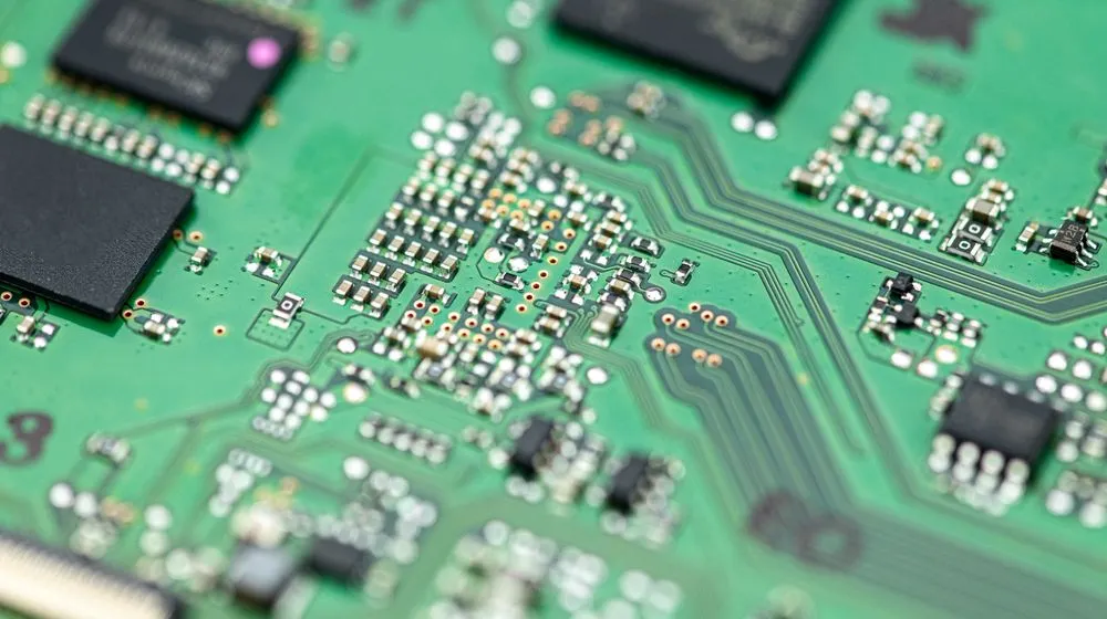
Copper pour refers to the process of filling unused areas of a printed circuit board (PCB) with copper, typically connected to ground or power planes. This technique is widely used to create a uniform copper distribution, which can help with heat dissipation, reduce electromagnetic interference (EMI), and simplify the etching process during manufacturing. It also provides a low-impedance return path for signals, which can be beneficial in many designs.
However, while copper pour has its advantages, it’s not a one-size-fits-all solution. Misusing it can lead to unexpected issues that degrade your PCB’s performance. Before we explore when to avoid copper pour, let’s look at the potential downsides that can arise if it’s not applied thoughtfully.
The Disadvantages of Copper Pour in PCB Design
While copper pour can be helpful, it comes with several disadvantages that designers must consider. These drawbacks can impact signal integrity, create noise issues, and complicate manufacturing. Here are some key copper pour disadvantages to keep in mind:
- Signal Coupling Risks: Copper pour, especially when placed near high-speed signal traces, can act as an unintended capacitor, leading to crosstalk or signal coupling. This can interfere with signal integrity, particularly in designs where signals operate at frequencies above 100 MHz.
- Noise Issues: If the copper pour isn’t properly connected to ground or if there are floating copper areas, it can act as an antenna, picking up or radiating noise. This is a common issue in mixed-signal designs where analog and digital signals coexist.
- Increased Parasitic Capacitance: A large copper pour near sensitive traces can introduce parasitic capacitance, altering the impedance of traces and potentially slowing down signal propagation. For example, a trace with a target impedance of 50 ohms might deviate by 5-10% due to unwanted capacitance from a nearby pour.
- Thermal Imbalance: While copper pour can help with heat dissipation, an uneven distribution can cause thermal hotspots during soldering, leading to component stress or board warpage.
- Manufacturing Complications: Excessive copper pour can create challenges during PCB fabrication, such as uneven etching or difficulties in maintaining consistent copper thickness across the board.
Understanding these risks is the first step to identifying when copper pour might harm your design. Let’s explore specific scenarios where avoiding copper pour is the smarter choice.
Key Scenarios Where Copper Pour Can Harm Your PCB
Not every PCB design benefits from copper pour. In certain situations, it can introduce more problems than it solves. Below are some critical scenarios where you should avoid using copper pour to prevent PCB design mistakes and ensure optimal performance.
1. High-Speed Digital Designs with Tight Signal Integrity Requirements
In high-speed digital circuits, signal integrity is paramount. Copper pour near high-speed traces can create parasitic capacitance and inductance, leading to signal coupling and crosstalk. For instance, in a design with differential pairs operating at 1 GHz, a nearby copper pour might increase crosstalk by 10-15%, causing data errors or signal degradation.
To avoid this, keep copper pour away from critical signal paths or use controlled impedance routing without additional copper in sensitive areas. If grounding is necessary, consider using via stitching to connect ground planes instead of a solid pour.
2. Mixed-Signal Designs with Analog and Digital Sections
Mixed-signal PCBs, which combine analog and digital components, are particularly sensitive to noise issues. A copper pour connected to a noisy digital ground can couple interference into the analog section, degrading performance. For example, in an audio amplifier circuit, noise from a digital ground pour could introduce a hum or distortion in the output signal, with noise levels potentially rising by 20-30 mV.
In such cases, it’s better to split ground planes for analog and digital sections and avoid copper pour in areas where noise coupling is a concern. Use careful grounding techniques, such as star grounding, to minimize interference.
3. Designs with High-Frequency RF Components
Radio frequency (RF) circuits are highly susceptible to EMI and noise. A copper pour, especially if not properly grounded, can act as an antenna, radiating or receiving unwanted signals. This can interfere with RF performance, reducing receiver sensitivity or causing signal loss. For instance, in a 2.4 GHz wireless design, a poorly implemented copper pour might increase noise floor levels by 5-10 dB.
For RF designs, avoid copper pour unless it’s part of a well-designed ground plane with proper via stitching. Ensure that any copper pour is tied to ground at multiple points to prevent floating sections that could resonate at RF frequencies.
4. Small or Dense PCBs with Limited Space
In compact PCB layouts, adding copper pour can lead to unintended shorts or manufacturing problems. For example, if the clearance between traces and the pour is too small (e.g., less than 0.2 mm), it might cause etching errors or short circuits during fabrication. This is a common PCB design mistake in densely populated boards where space is at a premium.
In such designs, prioritize precise trace routing and component placement over adding copper pour. If copper balancing is needed for manufacturing, consult with your fabrication partner to determine the minimum clearance rules and whether pour is necessary.
5. Designs Prone to Thermal Imbalance During Assembly
Copper pour can help with heat dissipation, but it can also create thermal imbalances during soldering if not distributed evenly. Large copper areas absorb more heat, potentially causing uneven reflow and cold solder joints on nearby components. For instance, a copper pour covering 70% of one side of the board might lead to a temperature difference of 20-30°C during reflow, risking component failure.
If your design involves high-power components or requires precise thermal management, consider avoiding large copper pours. Instead, use thermal vias or heat sinks to manage heat without disrupting the soldering process.
Common PCB Design Mistakes Related to Copper Pour
Even when copper pour is used with good intentions, certain PCB design mistakes can amplify its disadvantages. Here are some frequent errors to watch out for:
- Floating Copper Pours: Leaving copper pour unconnected to ground or power creates floating conductors that can pick up noise or cause EMI. Always ensure pours are tied to a reference plane with vias.
- Inadequate Clearance: Placing copper pour too close to signal traces (e.g., less than 0.3 mm) increases the risk of signal coupling and manufacturing defects. Follow design rules for minimum spacing.
- Overuse in Sensitive Areas: Adding copper pour without considering the impact on high-speed or analog signals can degrade performance. Be selective about where pour is applied.
- Ignoring Manufacturing Constraints: Excessive copper pour can lead to uneven etching or plating issues during fabrication. Balance copper distribution to avoid manufacturing problems.
By avoiding these mistakes, you can minimize the risks associated with copper pour and ensure a more reliable PCB design.
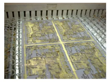
Manufacturing Problems Caused by Copper Pour
Beyond design challenges, copper pour can also introduce manufacturing problems that affect the quality and cost of your PCB. Here are some issues to consider:
- Uneven Etching: Large copper pours can result in uneven etching during fabrication, as the etchant may remove copper at different rates across the board. This can lead to inconsistent trace widths or weak connections.
- Copper Thickness Variations: Excessive pour can cause variations in copper thickness, especially in multilayer boards, making it harder to achieve uniform plating and potentially increasing production costs.
- Drilling and Via Issues: If vias are placed too close to a copper pour without proper clearance, it can lead to shorts or drilling errors during manufacturing.
To avoid these manufacturing problems, work closely with your fabrication team to understand their capabilities and constraints. Limit copper pour to areas where it’s necessary, and ensure that design rules for spacing and copper balance are followed.
Best Practices for Using Copper Pour Wisely
While there are scenarios where copper pour should be avoided, it can still be useful if applied correctly. Here are some best practices to minimize its disadvantages:
- Use Copper Pour Selectively: Only apply pour in areas where it serves a specific purpose, such as grounding or thermal management, and avoid it near high-speed or sensitive traces.
- Implement Proper Grounding: Ensure that all copper pours are connected to ground or power with multiple vias to prevent floating sections that can cause noise issues.
- Maintain Adequate Clearance: Follow design rules for spacing between copper pour and traces (e.g., at least 0.2-0.3 mm) to reduce signal coupling and manufacturing risks.
- Simulate and Test: Use simulation tools to analyze the impact of copper pour on signal integrity and EMI before finalizing your design. Test prototypes to validate performance.
By following these guidelines, you can harness the benefits of copper pour while avoiding common pitfalls that harm your PCB.
Conclusion: Make Informed Decisions About Copper Pour in Your PCB Designs
Copper pour can be a valuable tool in PCB design, but it’s not always the right choice. In scenarios involving high-speed signals, mixed-signal circuits, RF components, dense layouts, or thermal management challenges, the disadvantages of copper pour—such as signal coupling, noise issues, and manufacturing problems—can outweigh its benefits. By understanding when to avoid copper pour and following best practices, you can prevent common PCB design mistakes and ensure your board performs reliably.
Take the time to evaluate your design’s specific requirements and constraints before adding copper pour. Work closely with your manufacturing team to balance copper distribution and address potential fabrication challenges. With careful planning, you can create robust PCB layouts that meet your performance goals without unnecessary risks.
At ALLPCB, we’re committed to supporting engineers with the tools and knowledge needed for successful PCB designs. Whether you’re navigating copper pour decisions or tackling other layout challenges, our expertise and resources are here to help you achieve optimal results.


