ALLPCB


If you're diving into the world of micro SMD (Surface Mount Device) creation, you might be wondering how unmounted stencils and fine-tuned designs can elevate your PCB (Printed Circuit Board) projects. In short, unmounted stencils offer flexibility and precision for applying solder paste, while fine-tuning your designs ensures optimal component placement and functionality for micro SMDs. This blog post will guide you through the essentials of using unmounted stencils, mastering micro stencils, and perfecting your PCB designs with actionable tips and insights. Let’s explore the process step by step to help you achieve flawless results in your next project.
What Are Unmounted Stencils and Why Use Them for Micro SMD Creation?
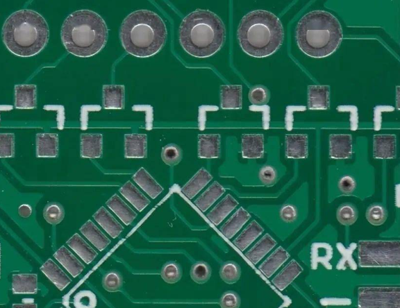
Unmounted stencils are thin sheets, often made of stainless steel, that are not fixed to a frame. Unlike framed stencils, which are pre-mounted for specific setups, unmounted stencils provide versatility for custom PCB layouts, especially when working with micro SMD components. These tiny components, often smaller than 1mm x 0.5mm, demand extreme precision in solder paste application, and unmounted stencils allow for tailored aperture designs to match unique board specifications.
The primary advantage of using unmounted stencils lies in their adaptability. You can cut, adjust, or align them to fit specific project needs, making them ideal for prototyping or small-batch production. Additionally, they are often more cost-effective than framed options, which is a significant benefit for hobbyists or small-scale engineers working on micro SMD designs. By using unmounted stencils, you ensure accurate solder paste deposition, reducing the risk of bridging or insufficient solder on tiny pads.
Getting Started with Micro Stencils: A Step-by-Step Tutorial
For those new to micro stencils, understanding how to use them effectively can make a huge difference in your PCB assembly process. This micro stencils tutorial will walk you through the basics to ensure precision and efficiency when working with SMD design placement.
Step 1: Design Your Stencil for Micro SMD Components
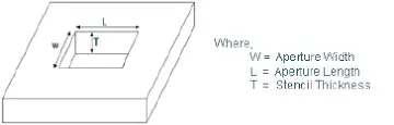
Start by creating a stencil design that matches your PCB layout. Use CAD software to define the apertures (openings) where solder paste will be applied. For micro SMD components, ensure the apertures are slightly smaller than the pad size—typically a 10-20% reduction in area—to prevent excess paste and potential short circuits. For instance, if your pad measures 0.8mm x 0.4mm, aim for an aperture of about 0.7mm x 0.35mm.
Step 2: Choose the Right Stencil Thickness
Stencil thickness is critical for micro SMDs. A thickness of 0.1mm to 0.12mm (4-5 mils) is often ideal for components with fine pitch (spacing between pins less than 0.5mm). Thicker stencils may deposit too much paste, while thinner ones might not provide enough for a reliable connection.
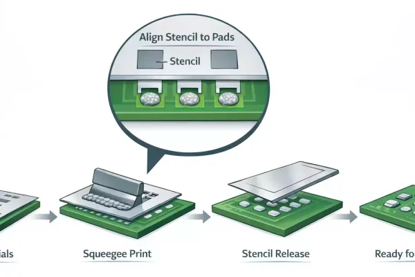
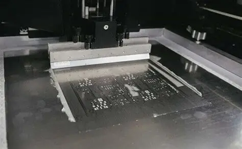
Step 3: Align and Secure the Unmounted Stencil
Since unmounted stencils aren’t framed, alignment is key. Use a jig or temporary adhesive to hold the stencil in place over your PCB. Ensure the apertures align perfectly with the pads to avoid misalignment, which can lead to soldering defects.
Step 4: Apply Solder Paste with Precision
Use a squeegee to spread solder paste across the stencil. Apply gentle, even pressure to push the paste through the apertures. For micro SMDs, a metal squeegee with a 45-degree angle often works best to achieve uniform deposition.
Step 5: Inspect and Clean
After applying the paste, lift the stencil carefully and inspect the PCB for consistency. Clean the stencil immediately with isopropyl alcohol and a lint-free cloth to prevent paste buildup, which can affect future applications.

Stencil Fine Tuning Tips for Optimal Results
Fine-tuning your stencil design and application process can significantly improve the quality of your micro SMD assemblies. Here are some stencil fine tuning tips to help you achieve precision and reliability in your projects.
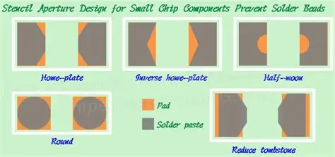
Adjust Aperture Shapes for Specific Components
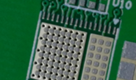
Not all micro SMD components have the same pad shapes or requirements. For instance, QFN (Quad Flat No-lead) packages may benefit from rounded aperture corners to reduce paste overflow, while rectangular pads for resistors might need a slight taper. Experiment with small adjustments in your design software to find the best fit for each component type.
Control Solder Paste Volume
Too much or too little solder paste can cause issues like tombstoning (components standing on end) or weak joints. Use a stencil thickness calculator or reference chart to match the paste volume to your component’s needs. As a rule of thumb, aim for a paste height of about 50-70% of the component’s standoff height after reflow.
Test with Small Batches First
Before committing to a large production run, test your stencil design on a small batch of PCBs. Check for issues like bridging (solder connecting adjacent pads) or insufficient paste. Adjust the aperture size or stencil thickness based on your findings.
Use High-Quality Solder Paste
The type of solder paste matters just as much as the stencil. Opt for a paste with fine particle size (Type 4 or 5) for micro SMDs, as it flows better through small apertures and provides cleaner results. Ensure the paste’s viscosity matches your application method for consistent performance.
PCB Creation Component Placement: Designing for Micro SMDs
When it comes to PCB creation component placement, micro SMDs present unique challenges due to their small size and tight spacing. A well-thought-out design is crucial to avoid manufacturing issues and ensure functionality. Here’s how to approach creation design components for success.
Prioritize Spacing and Orientation
Micro SMDs often have pitches as small as 0.4mm or less. To prevent soldering defects, maintain adequate spacing between components—at least 0.2mm for fine-pitch devices. Additionally, orient components to minimize signal interference and ease assembly. For example, align capacitors and resistors in the same direction to streamline pick-and-place processes.
Optimize Pad Design
Pad design directly impacts soldering quality. For micro SMDs, use pads that are slightly larger than the component’s footprint (about 0.1mm extra on each side) to account for placement tolerances. Ensure the pad’s solder mask opening is precise to avoid exposing adjacent traces, which could lead to shorts.
Consider Thermal Management
Micro SMDs, especially power components, can generate significant heat in a small area. Incorporate thermal vias or larger copper pours under components like LEDs or ICs to dissipate heat. For example, a thermal via grid with a 0.3mm diameter and 1.2mm pitch can improve heat transfer by up to 30% in high-density designs.
Account for Reflow Profiles
Your PCB design should align with the reflow soldering process. Group components with similar thermal mass together to ensure even heating. Avoid placing micro SMDs near large components that might create thermal shadows, leading to uneven solder melting.
Advanced Techniques for Fine-Tuning Micro SMD Designs
Beyond the basics, there are advanced strategies to fine-tune your designs for micro SMD creation. These techniques can help you tackle complex projects with confidence.
Leverage Design Rule Checks (DRC)
Use your PCB design software’s DRC tools to catch potential issues before fabrication. Set rules for minimum trace width (e.g., 0.1mm for high-density boards), clearance (at least 0.15mm between traces), and pad-to-pad spacing. Running a DRC can prevent costly errors during assembly.
Incorporate Fiducial Marks
Fiducial marks are small reference points on your PCB that help align the stencil and components during assembly. Place at least three fiducials (1mm diameter circles) near the corners of your board to ensure precise stencil alignment, especially for unmounted stencils.
Simulate Signal Integrity
For high-speed micro SMD designs, signal integrity is critical. Use simulation tools to analyze impedance and crosstalk. Aim for controlled impedance traces (e.g., 50 ohms for single-ended signals) by adjusting trace width and dielectric thickness. For instance, a 0.15mm wide trace on a 1.6mm FR4 board typically achieves 50-ohm impedance at 1 GHz.
Common Challenges and How to Overcome Them
Working with unmounted stencils and micro SMDs isn’t without challenges. Here are some common issues and solutions to keep your projects on track.
Misalignment of Stencil and PCB
Misalignment can lead to solder paste being applied incorrectly. Use alignment pins or a custom jig to hold the unmounted stencil in place. Double-check alignment under a magnifying glass before applying paste.
Solder Bridging on Fine-Pitch Components
Bridging occurs when excess paste connects adjacent pads. Reduce aperture size by 10-15% or switch to a thinner stencil (0.1mm) to control paste volume. Additionally, ensure your reflow profile ramps up slowly to allow paste to settle before melting.
Component Shifting During Reflow
Micro SMDs can shift if the solder paste isn’t balanced or if airflow in the reflow oven is uneven. Use a symmetrical pad design and apply paste evenly. If possible, secure the PCB on a flat, stable surface during reflow to minimize movement.
Conclusion: Mastering Micro SMD Creation with Unmounted Stencils
Creating high-quality PCBs with micro SMD components requires precision, patience, and the right tools. Unmounted stencils offer a flexible and cost-effective solution for applying solder paste with accuracy, while fine-tuning your designs ensures optimal component placement and performance. By following the steps in this micro stencils tutorial, applying stencil fine tuning tips, and focusing on PCB creation component strategies, you can elevate your projects to a professional level.
Whether you’re a hobbyist or a seasoned engineer, mastering these techniques will help you tackle even the most intricate designs with confidence. Start small, test often, and refine your approach with each project to achieve consistent, reliable results in SMD design placement and beyond.