 ALLPCB


Stencil printing is a critical step in PCB assembly, especially when working with bottom-terminated components (BTCs) like Quad Flat No-Lead (QFN) packages. However, achieving consistent results can be challenging due to issues like solder bridging, insufficient paste deposition, and voiding. In this comprehensive guide, we’ll explore the common stencil printing challenges with BTCs, provide actionable solutions for SMT assembly, and help you optimize your process for better outcomes in PCB production.
Whether you're dealing with QFN stencil printing or other BTC components, understanding these hurdles and how to overcome them is key to ensuring high-quality assemblies. Let’s dive into the details of stencil printing in SMT assembly and uncover practical tips to address these challenges.
What Are Bottom-Terminated Components (BTCs) and Why Are They Challenging?
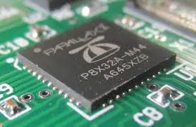
Bottom-terminated components, or BTCs, are a category of surface-mount devices where the electrical connections (terminals) are located on the bottom surface of the component. Common examples include QFN packages, Land Grid Arrays (LGAs), and other leadless components. These parts are widely used in modern electronics due to their compact size, excellent thermal performance, and ability to support high-density PCB designs.
However, BTCs pose unique challenges during stencil printing in SMT assembly. Unlike traditional components with visible leads, BTCs have hidden terminals, making it difficult to inspect solder joints after reflow. Additionally, their design often includes large ground planes or thermal pads, which require precise solder paste application to avoid defects like voiding or bridging. Poor stencil printing can lead to unreliable connections, reduced thermal performance, or even complete assembly failure.
Key Stencil Printing Challenges with BTC Components
Stencil printing is the process of depositing solder paste onto a PCB using a metal stencil with precisely cut apertures. While this step is critical for all SMT assemblies, BTC components introduce specific difficulties. Below, we break down the most common challenges faced during stencil printing for BTCs.
1. Solder Paste Bridging
One of the most frequent issues with BTCs, especially QFN packages, is solder paste bridging. This occurs when excess solder paste connects adjacent pads or terminals, creating unwanted electrical shorts after reflow. Bridging is often caused by stencil apertures that are too large or a stencil thickness that deposits more paste than needed. For fine-pitch QFN components with a pitch of 0.4mm or less, even a slight over-deposition can lead to this defect.
Impact: Bridging can cause short circuits, leading to functional failures in the assembled PCB. Detecting these issues can be difficult since BTC terminals are hidden under the component body.
2. Insufficient Solder Paste Deposition
On the flip side, insufficient solder paste can result in open connections or weak solder joints. This often happens when stencil apertures are too small or when the stencil thickness is inadequate for the component’s requirements. For BTCs with large thermal pads, insufficient paste can also hinder heat dissipation, impacting the component’s performance and longevity.
Impact: Weak or open joints can lead to electrical failures and reduced reliability, especially in high-stress applications.
3. Voiding in Large Ground Planes
Many BTCs, particularly QFNs, feature large central ground planes or thermal pads that require a significant amount of solder paste. During reflow, trapped air or flux volatiles can create voids—empty spaces within the solder joint. Voiding is a major concern as it reduces the thermal and electrical conductivity of the joint, potentially causing overheating or signal integrity issues.
Impact: High voiding rates (above 25% of the joint area, as per industry standards like IPC-7093) can compromise the component’s performance, especially in power-intensive applications.
4. Stencil Design and Alignment Issues
The design and alignment of the stencil are critical for accurate solder paste deposition. Misaligned stencils or poorly designed apertures can lead to uneven paste application, exacerbating issues like bridging or insufficient paste. For BTCs, where precision is paramount, even a small misalignment can cause significant defects.
Impact: Misalignment can result in inconsistent solder joints, leading to rework or scrap, which increases production costs.
Factors Contributing to Stencil Printing Challenges
Several factors influence the success of stencil printing for BTC components. Understanding these elements can help you identify the root causes of issues in your SMT assembly process.
Stencil Thickness and Aperture Design
Stencil thickness directly affects the amount of solder paste deposited. For fine-pitch QFN components (pitch below 0.4mm), a thinner stencil (0.12mm to 0.13mm) is often recommended to prevent over-deposition. For larger pitch components (above 0.4mm), a thicker stencil (0.15mm to 0.2mm) may be needed to ensure sufficient paste volume. Aperture design also plays a role—oversized or undersized openings can lead to bridging or insufficient paste, respectively.
Solder Paste Properties
The type of solder paste used, including its particle size and viscosity, impacts printability. For BTCs, finer particle sizes (Type 4 or Type 5) are often preferred for fine-pitch applications to ensure clean deposition through small apertures. Additionally, the paste’s flux chemistry can influence voiding during reflow.
Printing Parameters
Printer settings such as squeegee pressure, speed, and separation speed affect paste transfer efficiency. Incorrect settings can cause paste to smear or fail to release properly from the stencil, leading to inconsistent deposits on BTC pads.
PCB and Component Design
The PCB layout and BTC design also contribute to printing challenges. For instance, a densely packed board with minimal spacing between components can make stencil design more complex. Additionally, BTCs with large thermal pads require specific stencil patterns (like windowpane designs) to manage paste volume and reduce voiding.
Solutions to Overcome Stencil Printing Challenges with BTCs
While stencil printing for BTC components can be tricky, several strategies can help you achieve consistent, high-quality results in PCB assembly. Below are practical solutions tailored to address the challenges discussed earlier.
1. Optimize Stencil Design
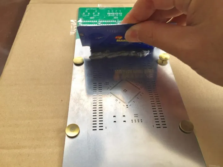
Work with your stencil manufacturer to customize aperture shapes and sizes based on the specific BTC components in your design. For QFN stencil printing, consider reducing aperture size by 10-20% compared to pad size to prevent over-deposition. For large thermal pads, use segmented or windowpane patterns to control paste volume and minimize voiding. Regularly inspect the stencil for wear or damage to ensure consistent performance.
2. Select the Right Stencil Thickness
Choose a stencil thickness that matches the pitch and requirements of your BTCs. As a general guideline, use 0.12mm to 0.13mm for fine-pitch components and 0.15mm to 0.2mm for larger pitch components. Testing different thicknesses during process development can help identify the optimal configuration for your assembly.
3. Fine-Tune Printing Parameters
Adjust your stencil printer settings to achieve uniform paste deposition. Experiment with squeegee pressure (typically 8-12 kg for most setups) and speed (20-40 mm/s) to find the best combination for your setup. Ensure proper stencil cleaning after every 5-10 prints to prevent paste buildup, which can cause defects.
4. Use High-Quality Solder Paste
Select a solder paste with appropriate particle size and flux chemistry for BTC applications. For fine-pitch QFNs, opt for Type 4 or Type 5 paste to ensure clean printing through small apertures. Additionally, choose a paste formulation designed to minimize voiding, especially for components with large thermal pads.
5. Implement Process Monitoring and Inspection
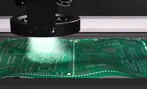
Use automated solder paste inspection (SPI) systems to detect issues like bridging or insufficient paste before reflow. SPI can measure paste volume and alignment, helping you catch defects early. Post-reflow, X-ray inspection is essential for BTCs since visual inspection cannot access hidden terminals. X-ray can identify voids and bridging, allowing for process adjustments.
Best Practices for QFN Stencil Printing in SMT Assembly
QFN components are among the most common BTCs, and their stencil printing process requires extra attention. Here are some best practices to ensure success:
- Pad Design: Follow manufacturer recommendations for pad sizing and thermal pad patterns. Avoid over-sizing pads, as this can lead to excess paste and bridging.
- Thermal Pad Stenciling: Use a windowpane or cross-hatch pattern for large thermal pads to reduce paste volume by 50-70%, minimizing voiding while ensuring adequate coverage.
- Reflow Profile: Optimize the reflow profile to allow proper outgassing of flux volatiles, reducing void formation. A longer soak zone (around 60-90 seconds at 150-180°C) can help.
- Stencil Cleaning: Clean the stencil regularly using an automated under-stencil wiping system with appropriate solvent to prevent paste residue from affecting print quality.
How to Minimize Voiding in BTC Solder Joints
Voiding is a persistent issue with BTCs due to their large thermal pads. While some voiding is inevitable, keeping it below 25% (as per industry standards) is critical for reliable performance. Here are targeted strategies to reduce voiding:
- Stencil Patterning: Use segmented apertures for thermal pads to control paste volume and promote even distribution.
- Solder Paste Selection: Choose low-voiding paste formulations with optimized flux chemistry for BTC applications.
- Reflow Optimization: Adjust the reflow profile to include a gradual ramp-up and extended soak time, allowing gases to escape before the solder solidifies.
- PCB Design: Incorporate vias in thermal pads to facilitate outgassing, but ensure they are tented or filled to prevent paste leakage.
Conclusion: Mastering Stencil Printing for BTC Components
Stencil printing challenges with bottom-terminated components like QFNs can significantly impact the quality and reliability of PCB assembly. Issues such as solder bridging, insufficient paste, and voiding are common but manageable with the right strategies. By optimizing stencil design, selecting appropriate materials, fine-tuning printing parameters, and implementing robust inspection processes, you can overcome these hurdles and achieve consistent results in SMT assembly.
At ALLPCB, we understand the complexities of working with BTC components and are committed to supporting your PCB assembly needs with tailored solutions. Whether you’re tackling QFN stencil printing or other BTC challenges, applying the tips and best practices outlined in this guide will help elevate your production quality and efficiency.
With careful attention to detail and a focus on process optimization, mastering stencil printing for BTCs is within reach. Keep refining your approach, and you’ll see improved outcomes in every assembly project.


