 ALLPCB


In the fast-evolving world of electronics manufacturing, precision is everything. For high-density printed circuit boards (PCBs), achieving flawless solder paste application is critical to ensure reliable connections and optimal performance. This is where nano-coating stencils come into play. These advanced tools improve solder paste release, reduce defects, and boost efficiency in PCB assembly. In this comprehensive guide, we’ll dive into how nano-coating stencils work, why they’re essential for high-density PCBs, and how they transform modern stencil technology.
What Are Nano-Coating Stencils and Why Do They Matter?
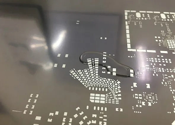
Nano-coating stencils are specialized tools used in surface mount technology (SMT) to apply solder paste onto PCBs. Unlike traditional stencils, these are treated with a ultra-thin layer of nano-coating material that enhances the release of solder paste from the stencil apertures. This results in cleaner, more precise deposits, especially on high-density PCBs where components are tightly packed, and pad sizes are incredibly small—often below 0.3 mm in width.
For manufacturers working with intricate designs, such as those found in smartphones, wearables, and IoT devices, nano-coating stencils are a game-changer. They minimize issues like bridging, insufficient solder, and stencil clogging, which can lead to costly rework or product failures. By improving solder paste release, these stencils ensure consistent results, even in the most challenging PCB assembly scenarios.
The Science Behind Nano-Coating Stencils
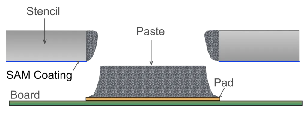
Nano-coating technology involves applying a microscopic layer—often just a few nanometers thick—of a hydrophobic or oleophobic material to the stencil surface. This coating reduces the surface tension between the stencil and the solder paste, allowing the paste to release more easily from the apertures. The result is a cleaner transfer of paste to the PCB pads, even for ultra-fine pitch components with spacing as tight as 0.2 mm.
Traditional stencils, often made of stainless steel, can struggle with paste adhesion, especially in high-density designs. The paste may stick to the walls of the apertures, leading to uneven deposits or voids. Nano-coatings address this by creating a slick surface that repels the paste, ensuring it transfers fully to the board. This technology also extends the life of the stencil by reducing wear and tear caused by frequent cleaning.
Challenges of Solder Paste Release in High-Density PCBs
High-density PCBs are packed with tiny components, often requiring solder paste deposits with volumes as low as 0.0001 cubic millimeters. Achieving this level of precision is tough due to several challenges:
- Small Aperture Sizes: As component sizes shrink, stencil apertures must also get smaller, increasing the risk of paste sticking inside the openings.
- Complex Designs: High-density boards often feature mixed technologies, with varying pad sizes and shapes, making uniform paste application difficult.
- Defects: Issues like bridging (solder connecting adjacent pads) or tombstoning (components standing upright) are more common in dense layouts if paste release isn’t perfect.
Nano-coating stencils tackle these problems head-on by ensuring smoother paste release, which directly translates to fewer defects and higher yield rates in production.
Benefits of Nano-Coating Stencils in PCB Assembly
Using nano-coating stencils offers several advantages for manufacturers aiming to perfect their PCB assembly process. Let’s break down the key benefits:
1. Improved Solder Paste Release
The primary advantage of nano-coating is its ability to enhance solder paste release. Studies have shown that nano-coated stencils can improve paste transfer efficiency by up to 30% compared to uncoated ones. This means more consistent deposits and fewer incomplete or uneven applications, even on pads smaller than 0.25 mm.
2. Reduced Defects and Rework
With better paste release, the likelihood of defects like bridging or insufficient solder drops significantly. This is crucial for high-density PCBs, where even a single defect can render an entire board unusable. Reducing rework saves time and cuts production costs.
3. Enhanced Stencil Durability
The nano-coating acts as a protective layer, minimizing wear on the stencil during repeated use and cleaning cycles. This can extend the lifespan of a stencil by up to 50%, depending on the coating quality and usage conditions.
4. Compatibility with Fine-Pitch Components
For boards with fine-pitch components (spacing below 0.4 mm), nano-coating ensures that solder paste is applied accurately without clogging or smearing. This precision is vital for maintaining signal integrity in high-speed circuits, where impedance mismatches can degrade performance.
5. Cost-Effective in the Long Run
While nano-coated stencils may have a higher upfront cost, their ability to reduce defects and extend stencil life makes them a cost-effective choice over time. Manufacturers often report a return on investment within months due to lower defect rates and less frequent stencil replacements.
How Nano-Coating Stencils Fit Into Modern Stencil Technology
Stencil technology has evolved rapidly to keep pace with the demands of modern electronics. Nano-coating is just one of many advancements, but it stands out for its impact on high-density PCB assembly. Other innovations, like laser-cut apertures with tighter tolerances (down to ±0.005 mm), complement nano-coatings by ensuring even greater accuracy.
In addition, nano-coating can be combined with other surface treatments, such as electropolishing, to further smooth the stencil walls and enhance performance. This synergy allows manufacturers to push the boundaries of what’s possible in SMT assembly, producing boards with component densities unimaginable just a decade ago.
Applications of Nano-Coating Stencils in High-Density PCBs
Nano-coating stencils are particularly valuable in industries where high-density PCBs are the norm. Some key applications include:
- Consumer Electronics: Smartphones, tablets, and wearables rely on compact, high-density boards with hundreds of components per square inch. Nano-coatings ensure flawless assembly for these devices.
- Automotive Electronics: Modern vehicles use complex control units with dense PCB layouts. Precision soldering is critical for safety and reliability in these systems.
- Medical Devices: From pacemakers to diagnostic equipment, medical electronics demand zero defects. Nano-coating stencils help achieve the required precision.
- IoT Devices: Internet of Things (IoT) products often feature tiny, power-efficient components on high-density boards, making nano-coated stencils a perfect fit.
In each of these sectors, the ability to apply solder paste accurately on small, densely packed pads directly impacts product quality and performance.
Best Practices for Using Nano-Coating Stencils
To get the most out of nano-coating stencils in PCB assembly, manufacturers should follow these best practices:
- Optimize Stencil Design: Work with designers to ensure aperture sizes and shapes are tailored to the specific board layout. For high-density PCBs, aspect ratios (aperture width to stencil thickness) should ideally be above 1.5 to prevent paste sticking.
- Use High-Quality Solder Paste: Pair nano-coated stencils with solder pastes that have the right viscosity and particle size (Type 4 or Type 5 for fine-pitch applications) to maximize release efficiency.
- Maintain Proper Cleaning: Although nano-coatings reduce paste adhesion, regular cleaning is still necessary. Use gentle, non-abrasive methods to avoid damaging the coating.
- Control Printing Parameters: Adjust squeegee pressure, speed, and angle during printing to match the stencil’s capabilities. Typical squeegee speeds range from 20 to 70 mm/s for optimal results.
- Monitor Environmental Conditions: Temperature and humidity can affect solder paste behavior. Aim for a controlled environment with temperatures between 20-25°C and humidity at 40-60%.
Following these guidelines ensures that nano-coating stencils perform at their best, delivering consistent results across production runs.
Future Trends in Nano-Coating and Stencil Technology
The future of nano-coating stencils looks promising as the demand for smaller, more powerful electronics continues to grow. Researchers are exploring new coating materials that could further reduce surface tension and improve paste release for even finer pitches—potentially below 0.1 mm. Additionally, advancements in automated stencil printing systems are making it easier to integrate nano-coated stencils into high-speed production lines.
Another exciting trend is the development of self-cleaning coatings that actively repel contaminants, reducing maintenance needs. While still in the experimental stage, such innovations could revolutionize PCB assembly by minimizing downtime and boosting throughput.

Conclusion: Why Nano-Coating Stencils Are Essential for High-Density PCBs
As electronics become smaller and more complex, the need for precision in PCB assembly has never been greater. Nano-coating stencils offer a powerful solution by enhancing solder paste release, reducing defects, and improving overall efficiency. Whether you’re producing cutting-edge consumer gadgets or critical automotive systems, this advanced stencil technology can elevate your manufacturing process to new heights.
By investing in nano-coated stencils and following best practices, manufacturers can tackle the challenges of high-density PCBs with confidence. The result is not just better products, but also significant cost savings and a competitive edge in a demanding market. At ALLPCB, we’re committed to supporting your success with the latest innovations in PCB assembly technology. Explore how nano-coating stencils can transform your production line today.


