 ALLPCB


In the fast-paced world of printed circuit board (PCB) manufacturing, ensuring quality is critical. One common issue that can compromise a PCB's functionality is solder bridge defects, where unintended connections form between components due to excess solder. Fortunately, AOI systems utilize image-based inspection technology to automatically detect and identify solder bridge defects, helping manufacturers maintain high standards and reduce errors. At ALLPCB, we understand the importance of precision, and in this blog, we’ll dive deep into how these systems work, their benefits, and why they are essential for modern PCB production.
What Are Solder Bridge Defects in PCB Manufacturing?
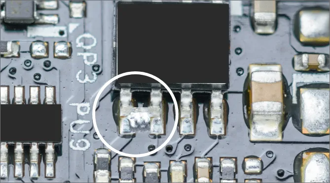
Solder bridge defects occur when excess solder creates an unintended connection between two or more points on a PCB, often between adjacent pads or pins. This can lead to short circuits, causing the board to malfunction or fail entirely. These defects are particularly common in high-density boards where components are closely packed, and even a tiny amount of misplaced solder can create significant issues.
Manually inspecting for such defects is time-consuming and prone to human error, especially as PCB designs become more complex. This is where Automated Optical Inspection (AOI) systems come into play, offering a reliable and efficient solution to detect and address solder bridge defects early in the production process.
What Are AOI Systems and How Do They Work?
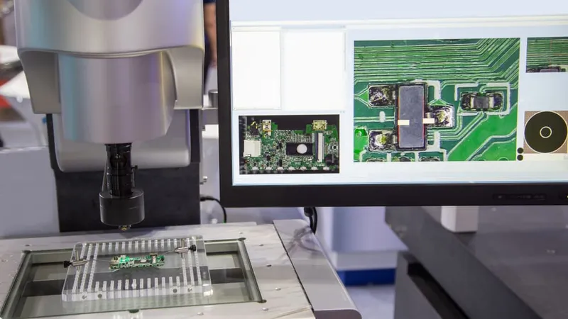
AOI systems are advanced tools used in electronics manufacturing to inspect PCBs for defects without human intervention. These systems rely on high-resolution cameras, specialized lighting, and powerful software algorithms to capture and analyze images of the board. By comparing the captured images to a reference design or predefined standards, AOI systems can quickly identify issues like solder bridges, missing components, or incorrect placements.
Here’s a breakdown of how AOI systems detect solder bridge defects using image-based inspection technology:
- Image Capture: High-resolution cameras take detailed images of the PCB surface, often under different lighting conditions to highlight specific features like solder joints.
- Image Processing: Software processes these images, enhancing details and identifying potential anomalies. For solder bridges, the system looks for unexpected connections or excess solder between pads.
- Defect Identification: The system compares the processed images against a “golden board” or design file. Any deviation, such as an unintended solder connection, is flagged as a defect.
- Reporting: Once a defect is detected, the system logs its location and type, allowing manufacturers to address the issue before the board moves further in production.
This automated process can inspect thousands of solder joints in seconds, far surpassing the speed and accuracy of manual inspection. For instance, some AOI systems can achieve defect detection rates of over 99%, significantly reducing the risk of faulty boards reaching the market.
Why Are AOI Systems Essential for Detecting Solder Bridge Defects?
Solder bridge defects can be incredibly small, sometimes less than 0.1mm in width, making them nearly invisible to the naked eye. Without proper inspection, these defects can lead to costly rework or, worse, product failures in the field. AOI systems offer several key advantages in tackling this issue:
1. High Precision and Accuracy
AOI systems utilize image-based inspection technology to automatically detect and identify solder bridge defects with unmatched precision. Their ability to zoom in on microscopic details ensures that even the smallest solder bridges are caught before they cause problems. Studies show that AOI systems can reduce false negatives by up to 90% compared to manual inspection.
2. Speed and Efficiency
In a high-volume production environment, speed matters. AOI systems can inspect an entire PCB in under 10 seconds, even for complex designs with thousands of solder points. This allows manufacturers to maintain throughput without sacrificing quality.
3. Cost Savings
Detecting defects early in the manufacturing process saves significant costs. Reworking a board after assembly or recalling a defective product can cost hundreds or thousands of dollars per unit. By catching solder bridge defects during production, AOI systems help avoid these expenses, improving overall profitability.
4. Consistency and Reliability
Unlike human inspectors, who may tire or miss defects due to fatigue, AOI systems deliver consistent results 24/7. They don’t overlook issues due to distraction or subjective judgment, ensuring every board meets the same high standards.
Types of Solder Bridge Defects AOI Systems Can Detect
Not all solder bridge defects are the same. AOI systems are designed to identify various types of issues related to soldering, including:
- Visible Solder Bridges: Excess solder that creates a visible connection between two pads or pins, often caused by over-application of solder paste or improper reflow.
- Hidden Solder Bridges: Bridges that form under components or in areas not easily visible, which AOI systems can detect using angled cameras or advanced imaging techniques.
- Micro Bridges: Tiny connections, sometimes less than 0.05mm, that require high-resolution imaging to identify. These are common in fine-pitch components.
- Intermittent Bridges: Defects that may not be consistent but can still cause failures under specific conditions, such as thermal expansion. AOI systems can flag potential risks even if the bridge isn’t fully formed.
By addressing these variations, AOI systems ensure comprehensive quality control across all stages of PCB assembly, from bare board inspection to post-reflow checks.
How AOI Systems Improve Overall PCB Quality
While detecting solder bridge defects is a primary function, AOI systems contribute to overall PCB quality in several other ways:
- Component Placement Verification: AOI systems check for correct component placement, ensuring no parts are misaligned or missing, which could indirectly contribute to soldering issues.
- Solder Joint Integrity: Beyond bridges, AOI can assess solder joint quality, identifying insufficient or excessive solder that might lead to weak connections or future failures.
- Traceability: Many AOI systems log inspection data for each board, providing full traceability. This is invaluable for identifying patterns in defects or improving processes over time.
- Reduced Manual Inspection: By automating defect detection, AOI systems free up skilled technicians to focus on more complex tasks, boosting overall productivity.
For example, a typical AOI system might inspect up to 50,000 solder joints per hour, catching defects that could lead to failure rates as low as 0.01% in final products. This level of quality control is essential for industries like automotive or medical electronics, where reliability is non-negotiable.
Challenges and Limitations of AOI Systems in Detecting Solder Bridges
While AOI systems are incredibly powerful, they are not without challenges. Understanding these limitations helps manufacturers use the technology effectively:
- Complex Geometries: In densely packed or multi-layered PCBs, shadows or overlapping components can obscure solder bridges, making detection harder. Advanced systems with 3D imaging are often needed for such cases.
- False Positives: Occasionally, AOI systems may flag non-issues as defects, requiring manual verification. Fine-tuning the software can minimize this, but it adds to setup time.
- Initial Cost: High-end AOI systems can be expensive to implement, with costs ranging from $50,000 to over $200,000 depending on features and capabilities. However, the return on investment through reduced defects often justifies the expense.
- Programming Complexity: Setting up an AOI system requires skilled technicians to program inspection parameters and update them for new designs, which can be time-intensive.
Despite these challenges, the benefits of AOI systems far outweigh the drawbacks, especially for high-volume or high-reliability PCB production.
Choosing the Right AOI System for Solder Bridge Detection
Selecting an AOI system for your manufacturing needs involves several considerations to ensure it effectively detects solder bridge defects:
- Resolution and Imaging Capabilities: Look for systems with high-resolution cameras (e.g., 5 megapixels or higher) and multi-angle lighting to capture clear images of solder joints.
- Software Features: Choose a system with advanced image-processing algorithms and customizable defect criteria to minimize false positives and negatives.
- Speed: Ensure the system can keep up with your production rate. For high-volume lines, look for systems capable of inspecting at least 30-50 boards per minute.
- Integration: Opt for AOI systems that integrate seamlessly with your existing manufacturing equipment and software for smooth data sharing and process control.
At ALLPCB, we prioritize partnering with manufacturers who leverage cutting-edge AOI technology to ensure the highest quality in every PCB we produce. Our commitment to precision helps deliver reliable boards for all your applications.
Future Trends in AOI Technology for PCB Inspection
As technology advances, AOI systems are becoming even more sophisticated in detecting solder bridge defects. Here are some emerging trends to watch:
- Artificial Intelligence (AI) Integration: AI-powered AOI systems can learn from past inspections, improving defect detection accuracy over time and reducing false positives by up to 30%.
- 3D Imaging: Traditional 2D AOI systems are being replaced by 3D models that provide depth information, making it easier to detect hidden solder bridges under components.
- Real-Time Analytics: Future AOI systems will offer real-time feedback during production, allowing immediate adjustments to soldering processes to prevent defects before they occur.
- Cost Reduction: As technology becomes more accessible, the cost of AOI systems is expected to decrease, making them viable for smaller manufacturers with tighter budgets.
These advancements promise to make AOI systems even more indispensable for PCB manufacturing, ensuring higher quality and efficiency in the years to come.
Conclusion: Elevating PCB Quality with AOI Systems
In the world of PCB manufacturing, solder bridge defects pose a significant risk to product reliability and performance. Thankfully, AOI systems utilize image-based inspection technology to automatically detect and identify solder bridge defects with precision, speed, and consistency. By integrating these systems into the production process, manufacturers can catch issues early, reduce costs, and deliver high-quality boards to their customers.
At ALLPCB, we are dedicated to leveraging the best inspection technologies to ensure every PCB meets the highest standards. Whether you’re producing simple prototypes or complex, high-density boards, AOI systems play a vital role in achieving flawless results. Trust us to support your projects with the quality and reliability you need for success.


