ALLPCB


Introduction
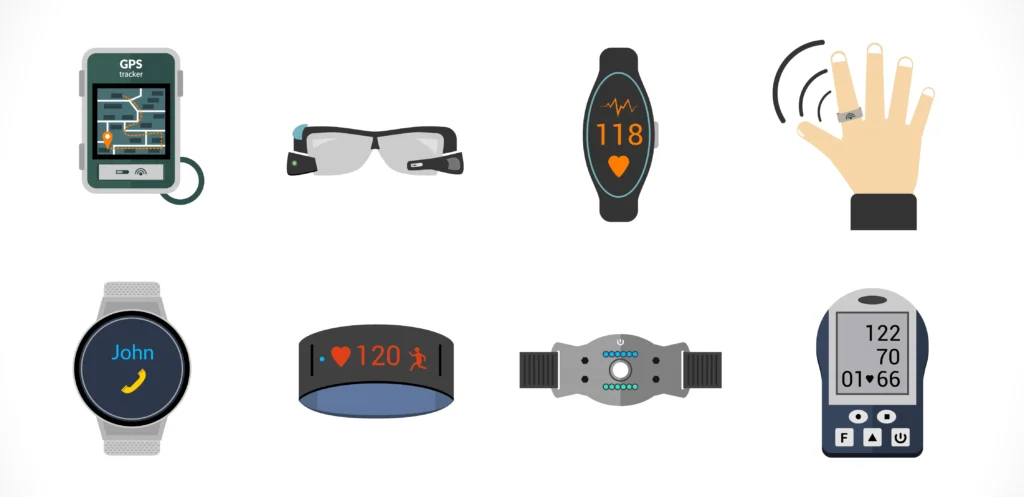
Circuit protection techniques and printed circuit board layout strategies help improve safety, reliability, and connectivity. Wearable technology has a vulnerability not typically found in other IoT devices: the human body generates static charge during movement. Electrostatic discharge (ESD) can damage the sensitive electronics that support IoT applications.
To understand this issue, start with the human body model (HBM) as applied to describing the sensitivity of integrated circuits to ESD damage. The commonly used HBM concept is defined in military standard MIL-STD-883, method 3015.8, for ESD sensitivity classification. A similar international HBM standard is JEDEC JS-001. Both JEDEC JS-001 and MIL-STD-883 use a 100 pF capacitor and a 1.5 kΩ discharge resistor to represent a charged human body. In testing, the capacitor is charged to voltages from 250 V to 8 kV and then discharged through the 1.5 kΩ resistor in series with the device under test.
Because wearable devices are designed for body contact, they are continually exposed to electrostatic events generated by close user interaction. Without appropriate protection, a wearable device's sensor circuits, battery charging interface, buttons, or data I/O ports can be damaged by ESD of a magnitude similar to HBM test events. A failure in a wearable device can affect the function and reliability of the wider IoT system that depends on it.
Applying circuit protection techniques and careful PCB layout early in the design process helps designers improve wearable device performance, safety, and reliability, and contributes to more reliable IoT systems.
1. Small packages, significant ESD protection
One design challenge for wearable device protection is the ongoing reduction in device size. Historically, protection required large discrete diodes and large package sizes. Designers now must balance the need for effective protection with the limited board area available in wearables.
Prefer unidirectional diode configurations where possible, because they perform better during negative-voltage ESD events. During a negative ESD event, the clamp voltage for a unidirectional diode is based on the diode forward drop (typically less than 1.0 V). In contrast, a bidirectional diode clamps based on reverse breakdown voltage during negative events, which is higher. Therefore, a unidirectional configuration significantly reduces stress on the system during negative ESD transients.
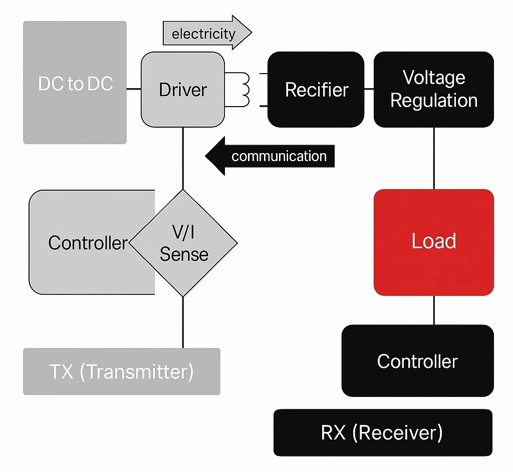
Place protection diodes carefully. Most wearable designs do not require board-level TVS diodes on every IC pin. Instead, identify pins that are exposed to potential user-contact ESD events. If users can touch communication or control lines, these lines can be entry points for ESD into integrated circuits. Typical vulnerable interfaces include USB, buttons or switch controls, and other data buses. Because adding discrete protection consumes PCB area, use devices that fit 0201 or 01005 packages where possible. For some wearable applications, space-saving multi-channel arrays are appropriate. Regardless of package type, place ESD suppressors as close as possible to the ESD source. For example, USB port protection should be located close to the USB connector.
Keep trace lengths short. Trace routing is critical when designing TVS diode protection for IC pins. Unlike lightning transients, ESD does not release large current over a long period. When handling ESD, move the charge from the protected circuit to the ESD reference point as quickly as possible.
The primary factors are the trace length from the signal to the ESD device and the length from the ESD device to ground, rather than trace width. To limit parasitic inductance, traces should be as short as possible. Parasitic inductance can cause inductive overshoot, a short voltage spike that, on long stubs, can reach several hundred volts. Recent package advances include uDFN profiles that can be placed directly on data lanes, eliminating the need for long stubs.
Understand the definitions of the human body model (HBM), machine model (MM), and charged device model (CDM). In addition to HBM, MM and CDM are test models used to describe the ESD tolerance of ICs used in portable or wearable devices. Some semiconductor suppliers consider the MM model obsolete and tend to follow HBM robustness and failure modes, although some vendors still use it. CDM is another alternative model. Unlike HBM, which simulates interaction between a human and an IC, CDM simulates an IC sliding and then contacting a grounded surface. Devices are charged to a specified voltage and survival is tested; if the device survives, testing proceeds at higher voltage levels until failure. CDM is standardized by JEDEC in JESD22-C101E.
Chips such as processors, memory, and ASICs may be characterized under one or more of these models. Semiconductor suppliers use these models during manufacturing to ensure circuit robustness. The current supplier trend is to lower on-chip test voltage levels to save die area and to comply with strict internal ESD policies.
Strict ESD policies that rely on lower on-chip protection can benefit suppliers, but system-level designers must still prevent field or user-induced ESD from causing failures in devices that are sensitive at the application level. To protect highly sensitive ICs, selected protection components must both withstand elevated electrostatic stress and provide sufficiently low clamp voltages. Consider the following parameters when evaluating ESD protection devices:
- Dynamic resistance: This parameter describes a diode's ability to clamp and divert an ESD transient to ground. It helps determine how low the resistor value is after the diode conducts. Lower dynamic resistance is better.
- IEC 61000-4-2 rating: TVS diode suppliers determine this rating by increasing ESD voltage until the diode fails. The failure point describes the diode's robustness. A higher rating is better. Some TVS diodes can reach contact discharge levels of 20 kV or 30 kV, well above the IEC 61000-4-2 level 4 contact discharge of 8 kV.
As the wearable market grows and new devices are developed, demand for circuit protection increases. Considering ESD protection and appropriate PCB layout early in the design process is increasingly important. Small circuit protection devices such as TVS diodes can effectively protect sensitive ICs inside wearables and help maintain system reliability.
Robust long-term tracking algorithm
The starting point of this algorithm study was that using existing tracking or detection algorithms independently cannot provide long-term tracking of the target. Kalal created an approach that combines tracking and detection algorithms to address issues such as target deformation and partial occlusion during tracking. An improved online learning mechanism continuously updates the tracker’s salient feature points and the detector’s target model.
In this system, to maintain stable tracking, a PD controller is introduced based on the ground robot's position in the image so the aircraft remains above the ground robot. The controller input is the pixel position at the center of the camera frame; the feedback is the actual captured position of the ground robot in the image. The control block diagram is adjusted experimentally to tune the PD parameters so the ground robot stays near the image center.
2.2 Height control algorithm
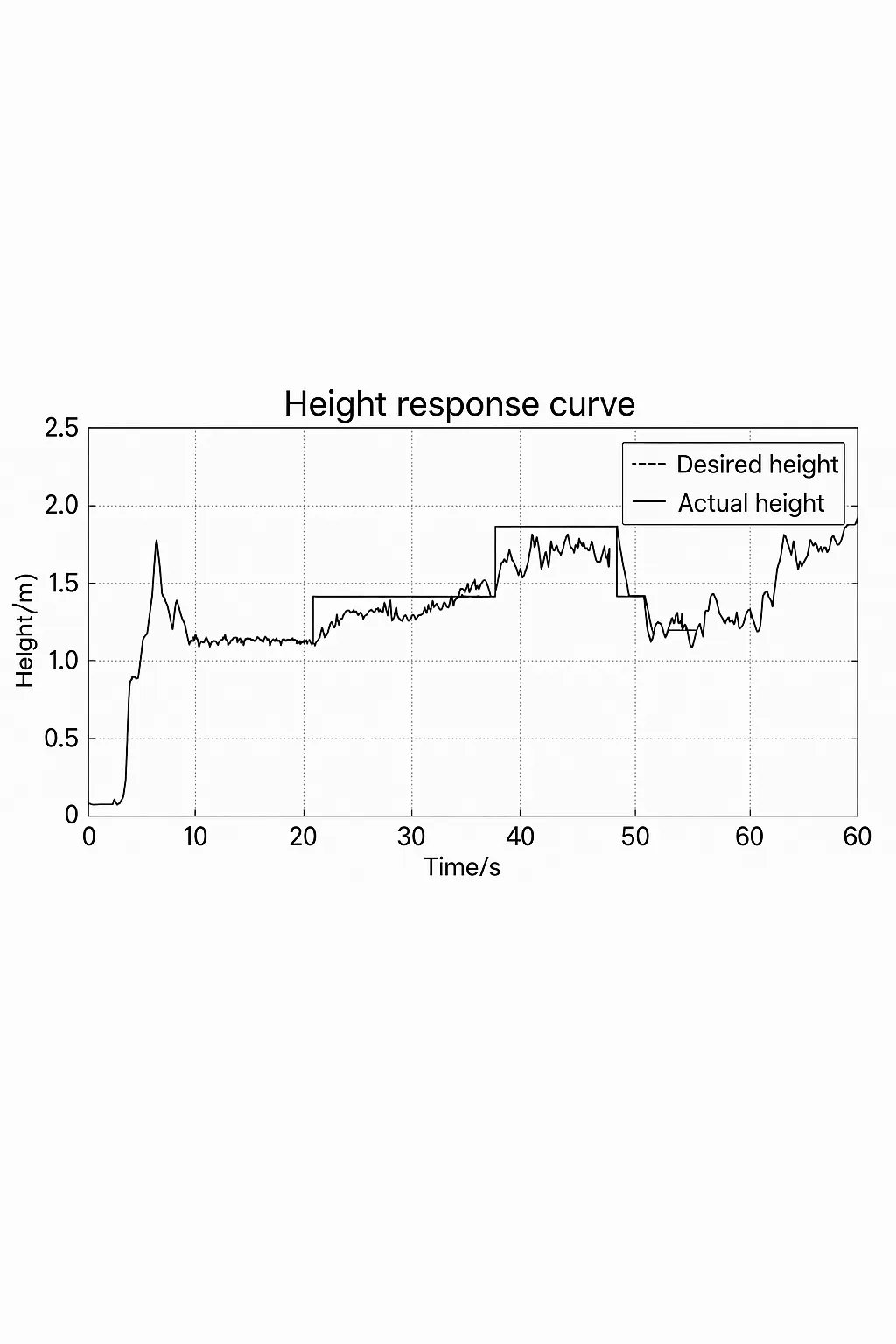
Based on actual aircraft experiments and the Wukong control system description, the throttle signal correlates with the aircraft's vertical motion. The throttle PWM duty-cycle count varies between 1000 and 2000; when between 1450 and 1550, the Wukong control system holds the aircraft at the current height. Based on this characteristic, a bang-bang (switch) controller was designed: when altitude is below the setpoint, set the duty-count to 1580 so the aircraft ascends slowly; when altitude is above the setpoint, set it to 1430 so the aircraft descends slowly. A deadband of ±5 cm around the setpoint disables control, effectively locking the current height. In experiments where the setpoint switched between 0.5 m, 1 m, and 1.5 m, the aircraft reached setpoints in a timely manner. During steering, the aircraft altitude changes and the controller adjusts accordingly. The straight line indicates the set height and the green line indicates actual aircraft altitude; the height controller was enabled near t = 10 s.
Conclusion
Based on the 7th-generation mission of the International Aerial Robotics Competition, this paper proposed a method for implementing an airborne system and described the hardware platform and software modules. The method accomplishes localization, altitude control, obstacle avoidance, and single ground-robot detection and tracking. Because aircraft flight endurance is limited and competition timing is constrained, higher-level strategy modules require further development to complete stage A pursuit tasks. Stage B introduces multiple aircraft interactions, so additional testing is needed to improve system robustness.