 ALLPCB


Introduction
Visual solder joint inspection under a microscope is a game-changer for electronic hobbyists building custom circuits or repairing gadgets. What looks fine to the naked eye often hides tiny flaws that cause intermittent failures or complete breakdowns later. A microscope reveals the true solder joint appearance, letting you spot issues before they ruin your project. This hands-on approach ensures reliable connections without fancy equipment. Hobbyists from beginners to advanced tinkerers benefit by catching problems early and improving their soldering skills over time.
Why Visual Solder Joint Inspection Matters for Hobbyists
Poor solder joints are behind most hobby projects that fail during testing or use. Heat, vibration, or power cycles stress weak spots, leading to opens, shorts, or unreliable signals. Using a visual solder joint inspection microscope helps you verify quality right after soldering, saving time on rework. It builds confidence in your assemblies and teaches you what good work looks like up close. Standards like IPC-A-610 provide criteria for acceptable joints, guiding hobbyists toward professional results even in home setups.
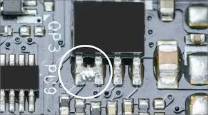
For hobbyists working on surface-mount devices or fine-pitch through-hole parts, naked-eye checks miss microcracks or incomplete wetting. Magnified inspection catches these early, preventing frustrating debug sessions. It also sharpens your eye for process improvements, like better flux use or iron temperature control.
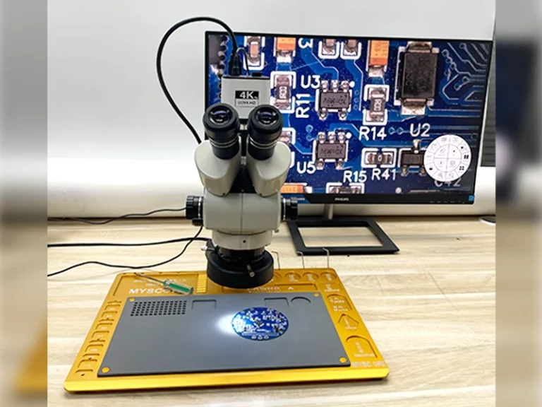
Choosing the Right Microscope and Magnification for Solder Joint Inspection
Start with a stereo microscope for its 3D depth perception, essential when inspecting uneven solder surfaces. Solder joint inspection magnification typically ranges from 10x to 50x, balancing detail and working distance. Lower settings around 10x to 20x suit broader views of chip components, while 30x to 50x zooms in on tiny pads or leads. Avoid ultra-high powers over 100x, as they narrow the field of view and make navigation tricky for hobbyists.
Good lighting is crucial, with adjustable LED rings to highlight surface texture without glare. Working distance should allow soldering iron access if you inspect mid-process. Digital USB microscopes work for budget setups, offering screen viewing and photo capture for later review. Test different magnifications on sample boards to find your sweet spot.
Ideal Solder Joint Appearance Under the Microscope
A good solder joint shines with a smooth, concave fillet that wets fully to the pad and lead. The surface looks mirror-like, free of dullness or graininess, indicating proper heating and flow. For surface-mount parts, the fillet rises evenly without spikes or balls. Through-hole joints show complete fill with a slight heel and toe curve matching the lead shape.
Examine wetting: solder must cover at least 75% of pad and lead surfaces for strength. No gaps or dewetting where solder pulls away. Color is bright silver, not darkened by overheating. These traits match criteria in standards like J-STD-001, ensuring mechanical and electrical reliability.
Under the microscope, tilt the board to check reflections, confirming uniformity. Consistent appearance across joints points to a solid soldering process.
Common Solder Joint Inspection Defects Under Microscope
Cold Joints
Cold joints appear rough and matte under the visual solder joint inspection microscope, lacking the shiny finish of proper reflow. They form from insufficient heat or movement during cooling, creating weak mechanical bonds. Cracks or grainy textures show clearly at 20x magnification. These fail under stress, causing intermittent connections in your circuits.
Solder Bridges
Bridges connect adjacent pads with unwanted solder globs, shorting signals. At higher solder joint inspection magnification, you see thin filaments or blobs spanning gaps. They often stem from excess flux or solder paste. Clean them promptly to avoid board damage during removal.
Voids and Blowholes
Voids are gas pockets inside the joint, visible as dark holes on the surface or fillet. Blowholes puncture from below, often flux-related. Inspect at 30x to gauge size; large ones weaken the joint per IPC-A-610 guidelines. Minimize by using fresh flux and controlled preheat.
Insufficient or Excess Solder
Insufficient solder leaves skinny fillets or exposed leads, risking opens. Excess forms elephant trunks or tombstones on chips. Balance volume during application for ideal coverage. Microscope views quantify these against pad sizes easily.
Cracks and Poor Wetting
Hairline cracks run along fillets from thermal shock or fatigue. Poor wetting shows solder balls or standoffs not adhering. These defects stand out under polarized light. Rework immediately to restore integrity.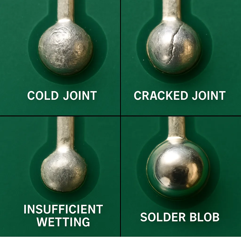
How to Use a Microscope for Soldering Inspection
Position your PCB flat under the microscope, starting at low magnification for overview. Adjust focus slowly while circling the board to check all angles. Use oblique lighting to reveal textures and shadows in solder joint appearance. For how to use microscope for soldering, keep one eye free or use a trinocular head for iron maneuvering.
Capture photos or videos during inspection for records and sharing in hobby forums. Calibrate scale if measuring fillet heights. Practice on scrap boards to build speed. Clean optics regularly for sharp images.
During live soldering, alternate between soldering and quick checks at 10x. This hybrid approach catches issues in real-time.
Best Practices for Effective Visual Inspection
Follow a systematic scan: start at board edges, move inward row by row. Note defect types and locations on a checklist. Reference IPC-A-610 images mentally for acceptance. Preheat boards gently to avoid new stresses during inspection.
Use magnification ladders: low for layout, high for details. Good ergonomics prevent eye strain, with adjustable stands and breaks. Document findings to track skill improvement.
Combine with multimeter tests post-inspection for full verification.
Troubleshooting Solder Joint Problems
If cold joints persist, raise iron temperature or dwell time. Bridges? Reduce solder amount and wick excess carefully. Voids suggest outgassing; try low-solids flux. Persistent cracks mean thermal mismatch; select compatible alloys.
For poor wetting, clean pads with IPA and freshen tips. Over time, analyze patterns to tweak your station setup. Hobbyist forums share similar fixes without gear specifics.
Conclusion
Mastering visual solder joint inspection under the microscope elevates your hobby projects from fragile prototypes to robust builds. Spotting good solder joint appearance versus defects like cold joints or bridges ensures longevity. Start with 10x-50x magnification and practical routines for quick wins. Reference standards like IPC-A-610 for pro-level criteria. With practice, you'll troubleshoot faster and solder better every time.
FAQs
Q1: What magnification is best for visual solder joint inspection microscope?
A1: For hobbyists, 10x to 30x works great for most SMD and through-hole joints, offering detail without losing context. Higher up to 50x helps tiny defects. Stereo models provide depth for accurate views. Adjust based on component size for efficient checks.
Q2: What are common solder joint inspection defects under microscope?
A2: Look for cold joints (dull, rough), bridges (unwanted connections), voids (holes), and cracks. Poor wetting shows gaps or balls. These appear clearly at 20x plus. Early detection prevents failures. Follow J-STD-001 for ideals.
Q3: How to use microscope for soldering inspection effectively?
A3: Set up with good lighting and 10x start magnification. Scan systematically, tilt for shadows. Inspect post-solder and mid-process if possible. Capture images for review. Practice builds speed and an eye for solder joint appearance.
Q4: What does good solder joint appearance look like under microscope?
A4: Shiny, smooth concave fillets with full pad and lead wetting. No dullness, gaps, or excess. Silver color, even shape per component type. Matches IPC-A-610 criteria for reliability.
References
IPC-A-610 — Acceptability of Electronic Assemblies. IPC.
J-STD-001 — Requirements for Soldered Electrical and Electronic Assemblies. IPC.


