 ALLPCB


Introduction
Solder joints form the backbone of any electronics project, connecting components to the printed circuit board (PCB) and ensuring reliable electrical performance. For electronic hobbyists, performing DIY solder joint inspection at home can prevent frustrating failures in circuits like amplifiers, sensors, or microcontrollers. Simple solder joint checks reveal issues early, saving time and materials during electronics troubleshooting. This guide focuses on practical, no-cost or low-cost methods using everyday tools. You will learn to identify common defects visually and with basic tests, aligning with industry benchmarks for quality. Mastering home solder joint inspection builds confidence in your soldering skills and project reliability.
What Are Solder Joints and Why Do They Matter?
A solder joint is the metallurgical bond between a component lead or pad and the molten solder alloy, typically tin-lead or lead-free compositions. Proper joints provide mechanical strength, electrical conductivity, and thermal dissipation essential for circuit operation. In hobbyist projects, poor joints lead to intermittent connections, overheating, or complete failures under vibration or power cycling. Regular basic PCB inspection catches these problems before they cause broader electronics troubleshooting headaches. Industry standards like IPC-A-610 define acceptable criteria for joint appearance and formation, helping hobbyists aim for professional-grade results. Inspecting joints routinely extends project lifespan and sharpens your assembly techniques.
Common Solder Joint Defects to Watch For
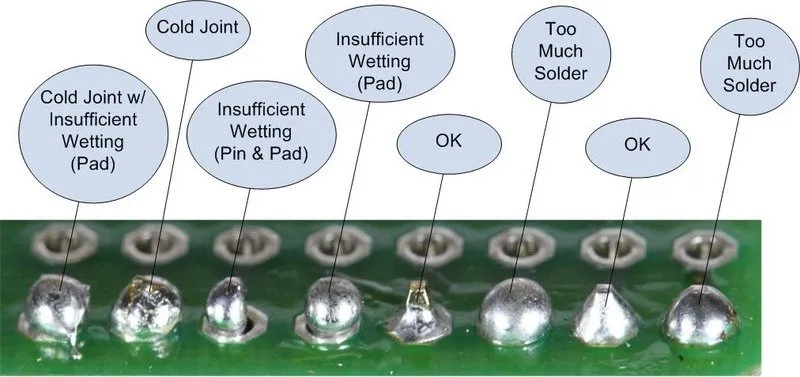
Cold solder joints appear dull, grainy, or lumpy because the solder did not fully melt or flow properly during cooling. These joints often show a rough surface without the smooth, shiny concave fillet that indicates good wetting to both the pad and lead. Insufficient heating or contaminated surfaces cause this defect, leading to high resistance and unreliable connections. In DIY projects, cold joints mimic opens during testing but may intermittently conduct.
Solder bridges occur when excess solder connects adjacent pads or pins unintentionally, creating shorts that bypass circuit paths. This common issue arises from applying too much solder or poor component alignment during hand soldering. Visually, bridges look like thin wires or blobs spanning multiple joints, potentially causing immediate power issues or erratic behavior. Spotting them early prevents complex electronics troubleshooting later.
Other frequent defects include tombstoning, where surface-mount components stand upright due to uneven reflow, and voids, which are gas pockets inside the joint reducing strength. Cracked joints from mechanical stress or thermal cycling show hairline fractures along the fillet edges. Excess solder forms bulbous mounds that hide underlying problems like poor wetting. Recognizing these through simple solder joint checks ensures robust hobbyist builds.
Essential Tools for Home Solder Joint Inspection
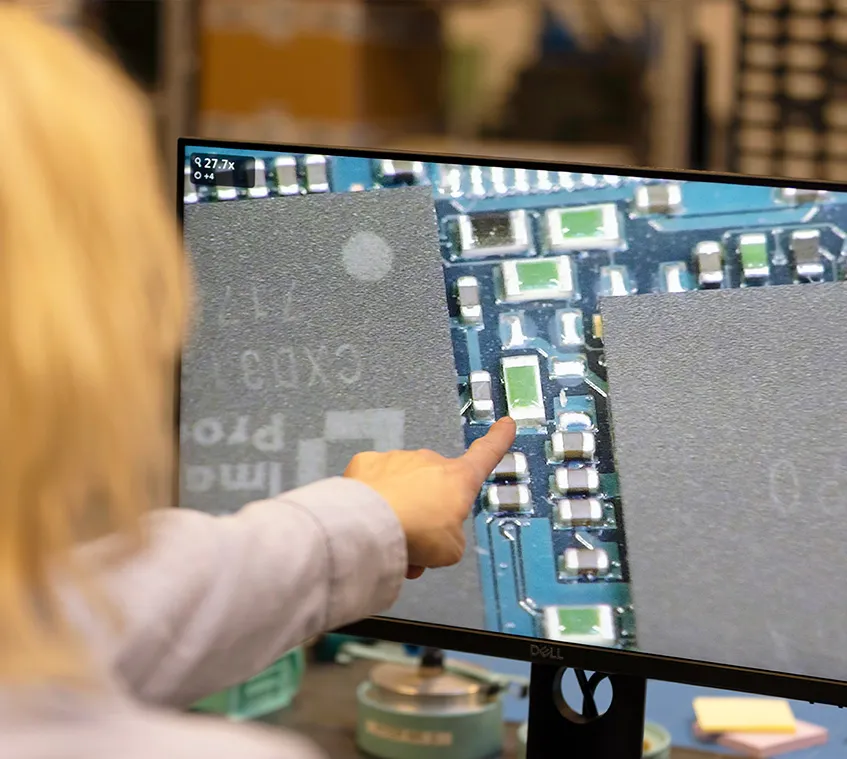
Start with a magnifying loupe or USB microscope offering 10x to 50x magnification for detailed views of joint fillets and pad wetting. Bright LED lighting, such as a desk lamp with adjustable focus, eliminates shadows and highlights surface textures. A digital multimeter measures continuity, resistance, and shorts between pins efficiently. Isopropyl alcohol and a soft brush clean flux residues that obscure defects during inspection.
For tactile feedback, use wooden toothpicks or plastic probes to gently nudge components without damage. Anti-static wrist straps protect sensitive parts during prolonged sessions. These basic items enable thorough DIY solder joint inspection without specialized equipment. Invest in quality magnification first, as it reveals 80 percent of issues visually.
Step-by-Step Guide to Simple Solder Joint Checks
Begin by powering off the circuit and discharging capacitors to ensure safety. Clean the PCB surface with isopropyl alcohol to remove flux and debris, improving visibility. Position the board under bright, angled lighting to cast shadows on joint contours.
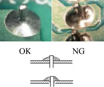
Examine each joint under magnification, checking for smooth, shiny fillets that wrap evenly around leads or pads. Verify the solder wets at least 75 percent of the pad surface without gaps or dewetting, as per acceptability criteria in standards like J-STD-001. Look for concave shapes with wetting angles under 90 degrees, indicating strong bonds. Rotate the board to inspect from multiple angles, catching hidden bridges or cracks.
Next, perform electrical tests with a multimeter set to continuity mode. Probe between adjacent pins for opens or shorts deviating from the schematic. Measure resistance across power rails to detect high values signaling poor joints. Gently flex the board while monitoring continuity to simulate real-world stress.
Document findings with photos before rework, noting defect types and locations. This systematic approach to basic PCB inspection streamlines electronics troubleshooting for hobbyists.
Advanced Visual Cues and What They Indicate
A good solder joint shines with a satin luster, forming a volcano-like shape for through-hole types or a straight fillet for surface-mount. Dull or matte appearances signal cold joints from rapid cooling or oxidation. Pitted surfaces suggest contaminated solder, while dewet areas show solder pulling away from pads due to oxides.
Bridge defects glisten if fresh but harden into rigid links, often with flux residue trails. Tombstoned parts lift one end, exposing bare pads underneath. Voids appear as dark spots in semi-transparent solder under strong backlighting. These cues, combined with IPC-A-610 guidelines, guide precise diagnosis.
Thermal stress indicators include lifted pads from overheating or cracking at joint heels. Compare against known good joints on the same board for consistency. Practice on scrap PCBs hones your eye for these subtleties in home solder joint inspection.
Practical Troubleshooting and Fixes for Defects
For cold joints, reheat with a fine-tip iron at 350 degrees Celsius, adding flux and fresh solder until smooth flow occurs. Avoid excessive dwell time to prevent pad damage. Solder bridges require desoldering braid or a vacuum pump to wick away excess material cleanly.
Tombstoning in surface-mount work often stems from uneven heating, so preheat the board next time with a hot air station or oven. Cracks demand component removal and reseating with fresh joints. Always test post-repair with multimeter and functional checks.
In electronics troubleshooting, isolate issues by dividing the circuit into sections. Poor joints cluster around heat-sensitive areas like voltage regulators. Reference J-STD-001 for process controls to prevent recurrence in future builds.
When to Seek Professional Help
Most defects yield to DIY fixes, but persistent intermittents or BGA packages exceed home capabilities. Multilayer boards with internal vias hide issues beyond visual reach. If failures recur despite inspections, consider assembly service for high-density projects.
Conclusion
DIY solder joint inspection empowers electronic hobbyists to achieve reliable circuits through simple solder joint checks and basic PCB inspection. Visual magnification, lighting, and multimeter tests spot cold joints, bridges, and more effectively. Adhering to principles from IPC-A-610 and J-STD-001 elevates your work to professional standards. Regular practice reduces electronics troubleshooting time and boosts project success. Start inspecting your next build today for dependable performance.
FAQs
Q1: What are the first steps in DIY solder joint inspection?
A1: Begin with cleaning the PCB using isopropyl alcohol to clear flux residues that hide defects. Use magnification and bright lighting to scan for shiny, smooth fillets on each joint. Perform continuity tests with a multimeter to confirm electrical integrity. This home solder joint inspection routine catches most issues early, preventing circuit failures during use.
Q2: How can I identify a cold joint during basic PCB inspection?
A2: Cold joints look dull, grainy, or lumpy without proper wetting to pads and leads. They fail to form the concave, shiny shape of good joints due to insufficient heat or contamination. Gently tug the component lead; loose fits confirm the defect. Rework by reheating with flux for reliable fixes in electronics troubleshooting.
Q3: What causes solder bridges and how to fix them in simple solder joint checks?
A3: Solder bridges form from excess material connecting adjacent pads, often during hand soldering misalignment. Spot them as thin shiny links under light. Remove with desoldering braid and fresh flux, then retest for shorts. Proper solder volume control prevents recurrence in hobbyist projects.
Q4: Is magnification necessary for effective home solder joint inspection?
A4: Yes, a 10x loupe or USB microscope reveals fillet details, wetting angles, and micro-cracks invisible to the naked eye. It aligns with industry visual criteria for accurate defect spotting. Combine with multimeter tests for complete electronics troubleshooting confidence. Basic tools make it accessible for all hobbyists.
References
IPC-A-610J — Acceptability of Electronic Assemblies. IPC, 2024
J-STD-001H — Requirements for Soldered Electrical and Electronic Assemblies. IPC, 2020


