ALLPCB


Via stubs represent an often overlooked yet critical factor in high-speed printed circuit board design. As signal frequencies continue to rise in modern electronics, the unused portions of plated through-holes can introduce unwanted reflections and distortions. Engineers working on multilayer boards must account for these effects early in the layout process to maintain reliable data transmission. Understanding via stubs helps prevent performance degradation that becomes evident only during testing or field operation.
What Are Via Stubs and Why They Matter
A via stub is the segment of a plated through-hole that extends beyond the layer where a signal trace connects, remaining electrically unused. In multilayer PCBs, this stub acts as a transmission line stub that can cause impedance discontinuities. At gigabit-per-second data rates, even short stubs create reflections that degrade signal integrity. The issue grows more pronounced as operating frequencies increase and board stackups become denser.
Via stubs signal integrity problems appear in applications such as servers, networking equipment, and high-performance computing systems. They contribute to eye diagram closure, increased bit error rates, and timing jitter. Designers who ignore these effects during layout often face costly respins after prototype validation. Addressing via stubs early supports compliance with performance targets and reduces the need for post-fabrication modifications.
Technical Principles and Mechanisms
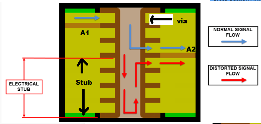
Signal propagation through a via follows transmission line theory. When a signal reaches the via, part of the energy continues along the intended path while the remainder travels into the stub. The stub reflects this energy back toward the source after a round-trip delay determined by its length and the propagation velocity of the dielectric. This reflected wave interferes with the original signal, producing ringing and overshoot.
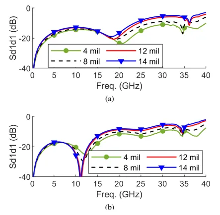
The severity depends on stub length relative to signal wavelength. Stubs shorter than one-tenth of the wavelength produce smaller effects, yet even modest lengths matter at multi-gigahertz frequencies. Dielectric constant, via diameter, and antipad size further influence the impedance mismatch. Modeling tools that solve Maxwell's equations help quantify these interactions during the design phase.
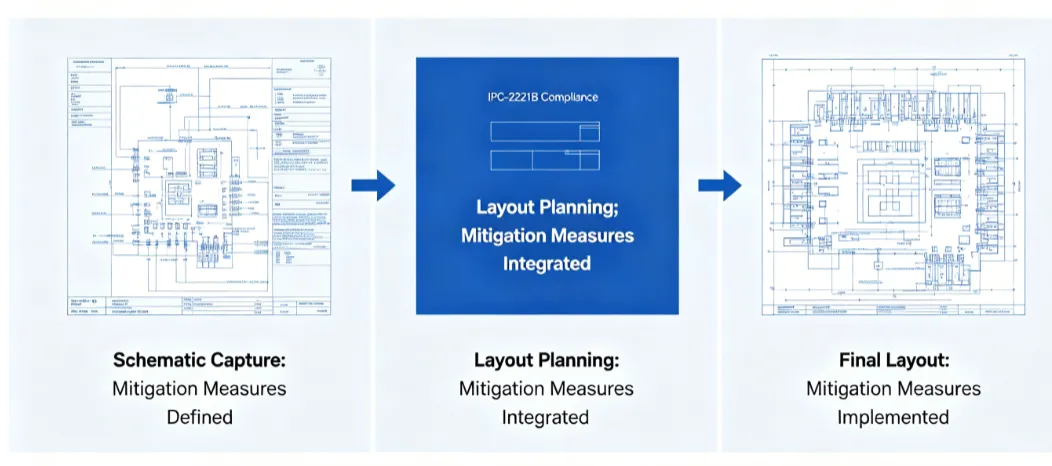
Industry standards such as IPC-2221 provide guidance on via sizing and placement to support controlled impedance. Proper application of these guidelines helps minimize initial discontinuities, although they do not eliminate the stub reflection mechanism itself.
Practical Solutions and Best Practices
Several layout strategies reduce via stub effects. One common approach uses blind or buried vias that terminate at the required layer without extending through the entire board thickness. This method eliminates the stub entirely but increases fabrication complexity and cost. Another technique involves careful layer assignment so that high-speed signals transition only between adjacent layers, keeping any remaining stub short.
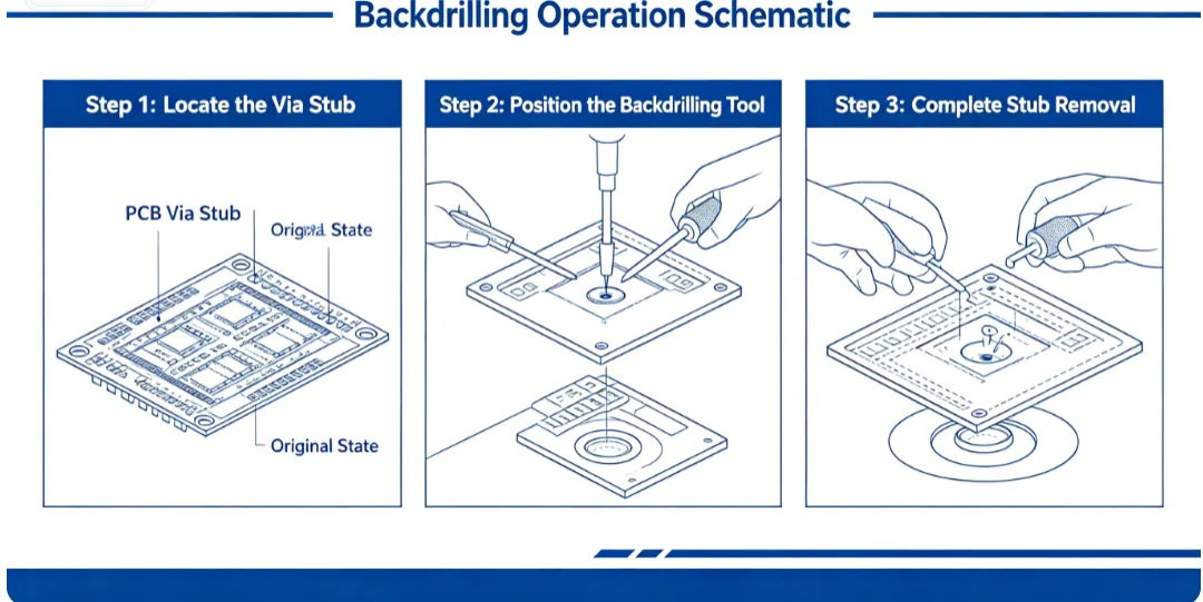
Backdrilling removes the unused via barrel after plating. The process drills from the opposite side to a controlled depth that stops just beyond the last used layer. Depth control must remain precise to avoid damaging functional connections. Designers specify backdrill locations on fabrication drawings and verify results through cross-section analysis.
Additional optimizations include adjusting via diameter, antipad size, and surrounding ground vias to improve return path continuity. Simulation of the full channel, including package and connector effects, validates that residual stubs stay within acceptable limits. Stacking multiple vias in series or using via-in-pad constructions can also shorten effective stub lengths when space permits.
Conclusion
Via stubs introduce reflections that compromise signal integrity in high-speed designs. Structured layout practices, appropriate via selection, and controlled-depth removal techniques address the root causes effectively. Early consideration during stackup definition and routing yields boards that meet performance requirements without extensive rework. Consistent application of these methods supports reliable operation across demanding applications.
FAQs
Q1: What causes via stubs signal integrity degradation in high-speed PCBs?
A1: Via stubs create impedance discontinuities that reflect portions of the propagating signal. The reflected energy interferes with the main waveform, increasing jitter and reducing eye opening. At higher frequencies the effect becomes measurable even with short stubs. Proper via selection and backdrilling limit these reflections to acceptable levels.
Q2: How does backdrilling vias improve signal integrity?
A2: Backdrilling removes the unused barrel segment after plating, shortening or eliminating the stub. The remaining via length matches the signal path more closely, reducing round-trip delay and reflection amplitude. Depth control during the secondary drilling operation determines the final stub length. This method works well for through-hole vias in dense multilayer boards.
Q3: When should designers consider via optimization instead of backdrilling?
A3: Via optimization through blind or buried constructions avoids stubs at the layout stage. This approach suits designs where fabrication cost allows and layer transitions stay within adjacent planes. Simulation confirms that residual discontinuities remain within budget before committing to production. Early stackup planning identifies opportunities for such optimizations.
Q4: What standards guide via design for signal integrity?
A4: IPC-2221 outlines via dimensioning and placement practices that support controlled impedance routing. Additional references such as IPC-6012 address qualification aspects of the finished board. These documents help establish baseline via geometries before detailed electromagnetic analysis.
References
- IPC-2221B — Generic Standard on Printed Board Design. IPC, 2012
- IPC-6012E — Qualification and Performance Specification for Rigid Printed Boards. IPC, 2017