 ALLPCB


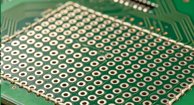
Via stitching connects multiple ground or power planes in a printed circuit board through an array of vias. This technique creates a low-impedance path that helps contain electromagnetic fields and supports stable return currents. Engineers apply via stitching in high-speed digital designs, RF circuits, and mixed-signal boards where electromagnetic interference must remain controlled. Proper spacing between these vias determines how effectively the stitched planes function as a continuous reference. When spacing aligns with operating frequencies, the board maintains signal integrity across layers.
Designers consider via stitching spacing early in layout because it influences both electromagnetic compatibility and overall board performance. The approach supports compliance with established qualification requirements for rigid printed boards.
What Is Via Stitching Spacing and Why It Matters
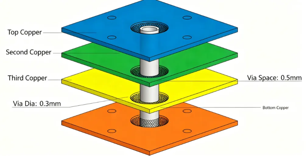
Via stitching spacing refers to the center-to-center distance between adjacent stitching vias that tie together copper planes. This distance directly affects the electrical continuity of the reference planes. In multilayer boards, stitching vias reduce the effective inductance of return paths and limit the formation of unintended slot antennas.
The practice matters because inadequate spacing allows high-frequency currents to radiate or couple into adjacent traces. Conversely, excessively dense stitching can increase manufacturing complexity without proportional performance gains. Engineers evaluate spacing during stack-up definition to balance electrical performance with fabrication constraints. Industry standards such as IPC-6012E guide the qualification of boards that incorporate such features.
Technical Principles of Via Stitching Spacing
Stitching vias function by providing multiple parallel paths for return current, thereby lowering the overall loop inductance between planes. When spacing exceeds a fraction of the wavelength at the highest frequency of interest, the planes begin to behave as discontinuous structures. This discontinuity can excite resonances that degrade noise margins and increase radiated emissions.
The mechanism involves the interaction between via inductance and the distributed capacitance of the planes. At higher frequencies, the via array must approximate a continuous sheet to prevent field leakage through gaps. Signal integrity suffers when return paths become elongated or when plane discontinuities create impedance variations along transmission lines.
Engineers analyze these effects using electromagnetic simulation to verify that the chosen spacing maintains plane integrity across the intended bandwidth. Thermal and mechanical considerations also enter the analysis because via density influences local stress during reflow and operation.
Effects of Via Spacing on Signal Integrity
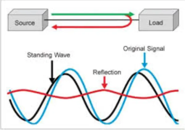
Via spacing influences signal integrity primarily through its impact on return-path inductance and crosstalk. When spacing is too large, high-speed signals experience increased ground bounce and simultaneous switching noise because return currents must travel farther to reach a stitching via. This lengthens the current loop and raises the effective inductance seen by the driver.
In differential pairs or single-ended traces routed over stitched planes, excessive spacing can also increase near-end and far-end crosstalk by allowing fields to couple through the gaps. At radio frequencies, the array can support propagating modes that radiate energy from board edges or connectors.
Designers therefore examine the frequency content of signals and the physical dimensions of the board when determining spacing. The goal remains to keep the maximum gap electrically small relative to the shortest wavelength present in the system.
Practical Guidelines for Optimum Via Stitching Spacing
Engineers begin by identifying the highest frequency component that must remain contained within the board. They then place stitching vias along the perimeter of each plane and around cutouts or slots that interrupt current flow. Additional vias are added near high-speed connectors and along the edges of power islands.
Spacing is chosen so that the array provides a sufficiently low-impedance mesh without exceeding fabrication limits on via density. In regions carrying sensitive analog signals, designers may tighten spacing locally while maintaining wider spacing in less critical areas.
Review of the board stack-up ensures that via aspect ratios remain within acceptable limits for plating quality. Thermal relief connections around stitching vias are avoided when maximum conductivity is required.
Best Practices in PCB Design
Layout teams integrate via stitching decisions into the initial floor-planning stage rather than adding them as an afterthought. They coordinate with fabrication partners to confirm that the selected spacing and via sizes align with the chosen manufacturing process.
Documentation includes clear notes on required via density and any keep-out zones around stitching features. Post-layout verification includes both electrical simulation and design-rule checks that flag excessive gaps between stitching vias.
When boards undergo qualification testing, the stitched planes contribute to meeting the performance criteria outlined in relevant IPC specifications.
Conclusion
Via stitching spacing forms a critical element of modern multilayer PCB design when electromagnetic containment and stable reference planes are required. Logical placement based on frequency content and board geometry yields measurable improvements in signal integrity and reduced emissions. Engineers achieve consistent results by following structured analysis, adhering to established qualification standards, and verifying layouts through simulation and review.
Attention to spacing early in the design cycle prevents costly iterations later in the product development process.
FAQs
Q1: What determines the optimum via stitching spacing in a PCB design?
A1: Optimum via stitching spacing depends on the highest frequency present in the system and the physical size of the copper planes. Engineers select spacing that keeps gaps electrically small relative to the operating wavelength while remaining compatible with manufacturing capabilities. The approach supports low-inductance return paths and helps maintain signal integrity across layers.
Q2: How does via spacing affect signal integrity in high-speed circuits?
A2: Via spacing directly influences return-path inductance and the continuity of reference planes. Larger spacing increases loop area for high-speed currents and can elevate crosstalk and ground bounce. Proper spacing minimizes these effects and preserves clean signal transmission.
Q3: When should designers apply via stitching spacing guidelines?
A3: Designers apply via stitching spacing guidelines during stack-up definition and initial layout of multilayer boards. The technique proves especially useful around connectors, plane cutouts, and board edges where electromagnetic fields must remain contained. Early implementation avoids later modifications that affect routing density.
Q4: Can via stitching spacing be adjusted after initial placement?
A4: Via stitching spacing can be refined after initial placement once simulation results or prototype measurements become available. Adjustments typically involve adding vias in areas showing elevated emissions or noise while preserving overall board manufacturability.
References
IPC-6012E — Qualification and Performance Specification for Rigid Printed Boards. IPC, 2017
IPC-A-600K — Acceptability of Printed Boards. IPC, 2020
JEDEC J-STD-020E — Moisture/Reflow Sensitivity Classification. JEDEC, 2014


