 ALLPCB


Via Stitching on a Budget: Low-Cost PCB Improvements
Via stitching offers a practical way to enhance PCB performance in affordable PCB design projects. Hobbyists often seek low-cost via techniques that improve signal integrity and reduce electromagnetic interference without requiring expensive fabrication runs. By placing additional vias strategically, designers connect copper layers more effectively while keeping overall board costs under control. This approach fits well with budget PCB tips that focus on layout optimization rather than added features. Many hobbyists achieve noticeable improvements simply by planning via placement during the initial design phase.
What Is Via Stitching and Why It Matters
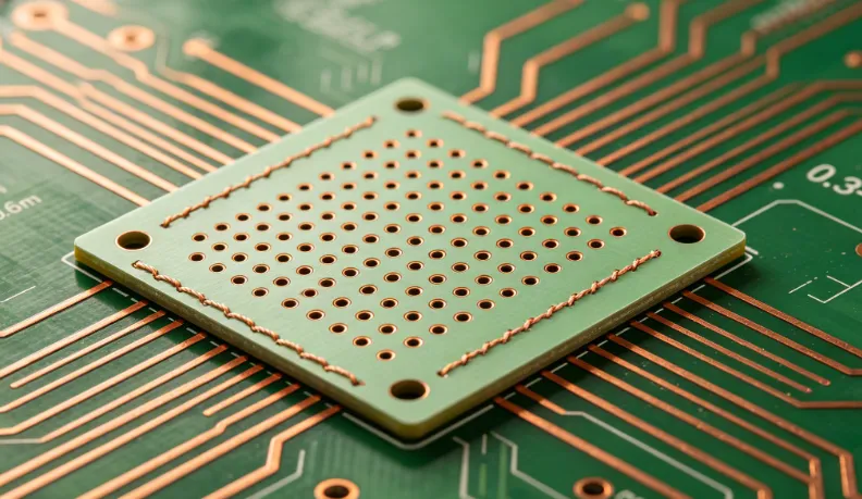
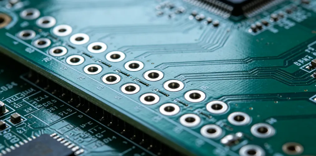
Via stitching involves adding multiple vias along a trace, plane, or board edge to create low-impedance connections between layers. In affordable PCB design, this technique helps maintain consistent ground references and provides better return paths for high-speed signals. Hobbyists working on radio frequency or mixed-signal boards find it especially useful because poor layer connections can lead to noise or performance issues. Low-cost via techniques allow these benefits without increasing the number of board layers or using specialized materials. Budget PCB tips emphasize using standard via sizes and spacing that most fabricators support at base pricing.
Industry standards such as IPC-2221 guide the minimum spacing and sizing requirements for vias in rigid boards. Proper application of these guidelines ensures reliability even in cost-sensitive projects.
Technical Principles Behind Via Stitching
Vias act as vertical conductors that link different copper layers in a multilayer board. When stitched together, they lower the overall inductance of ground or power planes and create a more effective shield against electromagnetic fields. In budget-conscious designs, the key is to distribute vias evenly rather than clustering them, which maintains performance while avoiding extra drilling charges. Signal return currents follow the path of least inductance, so stitched vias reduce loop areas that could otherwise radiate noise.
Thermal considerations also play a role. Additional vias can help dissipate heat from components, though hobbyists must balance this against the added copper area that affects etching costs. Low-cost via techniques focus on vias sized between 0.3 mm and 0.6 mm diameter, which most standard processes handle efficiently. These sizes provide adequate current capacity for typical hobbyist applications without requiring thicker copper or special plating.
Practical Solutions and Best Practices for Low-Cost Implementation
Start by reviewing the board stackup early in the design process. Identify ground planes or critical traces that would benefit from stitching and place vias at regular intervals, typically every 5 to 10 mm along edges or near high-speed lines. This spacing provides effective shielding while staying within standard fabrication tolerances. Use the same via size throughout the board to simplify drilling and reduce setup fees.
In affordable PCB design, avoid unnecessary stitching in low-speed areas where a single via suffices. Instead, concentrate vias near connectors, power entry points, and sensitive analog sections. Budget PCB tips include running a design rule check focused on via-to-via clearance and annular ring size to prevent manufacturing issues. Many hobbyists also route ground pours with stitching vias at the pour boundaries to maintain continuity across splits or cutouts.
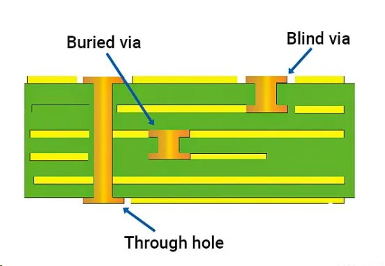
Another effective approach is to use via-in-pad only where component density demands it, and rely on standard through-hole vias elsewhere. This keeps costs low while still achieving the desired electrical performance. Always verify that the chosen via aspect ratio stays within the fabricator’s standard capabilities, usually under 8:1 for reliable plating.
Conclusion
Via stitching delivers meaningful improvements in signal quality and EMI performance when applied thoughtfully to affordable PCB design. Low-cost via techniques center on strategic placement, standard sizes, and adherence to basic spacing rules rather than excessive via counts. Hobbyists who incorporate these budget PCB tips during layout planning often see better results without increasing fabrication expenses. Consistent application of these practices supports reliable boards suitable for a wide range of projects.
FAQs
Q1: How does via stitching support affordable PCB design?
A1: Via stitching improves ground continuity and reduces noise using standard fabrication processes. Hobbyists can achieve these gains by adding vias at key locations without changing board thickness or copper weight. This keeps costs low while enhancing overall board performance.
Q2: What low-cost via techniques work best for hobbyist projects?
A2: Effective low-cost via techniques include using 0.4 mm to 0.6 mm diameter vias spaced 5 to 10 mm apart along ground planes. Designers focus on critical areas such as board edges and near connectors rather than uniform coverage. These choices align with typical budget fabrication options.
Q3: Can via stitching be added after initial layout without major cost increases?
A3: Yes, minor adjustments to via placement during final review usually incur little or no extra cost. Hobbyists review the design for stitching opportunities near high-speed traces and ground returns before sending files for production. This step fits easily into standard budget PCB tips.
Q4: Does via stitching affect thermal performance in budget boards?
A4: Stitched vias can provide additional heat paths when placed near power components. However, the primary goal remains electrical connectivity, so thermal benefits appear as a secondary advantage in most hobbyist applications. Careful placement avoids unnecessary copper that could raise etching costs.
References
IPC-2221 — Generic Standard on Printed Board Design. IPC.
IPC-6012E — Qualification and Performance Specification for Rigid Printed Boards. IPC, 2017.
IPC-A-600K — Acceptability of Printed Boards. IPC, 2020.


