 ALLPCB


Introduction
If you are new to PCB design for beginners, you have likely encountered the challenge of fitting more electronic components into a smaller space. Vias play a key role in multilayer boards by connecting traces across different layers. Among various via types, via-in-pad stands out as a technique that integrates the via directly into a surface mount pad. This approach is especially useful for high-density designs where space is at a premium. In this via-in-pad tutorial for beginners, we will break down the basics step by step. By the end, you will understand how to incorporate it into your projects without overwhelming complexity.
The relevance of via-in-pad grows with the trend toward smaller, more powerful devices. Hobby projects often involve ball grid array components or fine-pitch packages that benefit from this technique. Without it, boards become larger and more prone to routing congestion. Manufacturers support via-in-pad to meet demands for higher integration levels. As you explore PCB design for beginners, recognizing when to use this feature prevents common layout pitfalls. Ultimately, it bridges the gap between simple prototypes and professional-grade boards.
What Is Via-in-Pad? Understanding the Basics
Via-in-pad refers to a PCB design feature where a via is placed precisely within the footprint of a surface mount pad, rather than offset to the side. This method allows the pad to serve dual purposes: mounting electronic components and providing interlayer connections. Traditional vias require extra space around pads, which can limit component density on boards with many electronic components. Via-in-pad eliminates this issue, making it ideal for modern electronics like smartphones or wearables that demand compact layouts. For electronic hobbyists, grasping via-in-pad basics means unlocking more efficient routing options. It also improves signal integrity by shortening paths between layers.
The relevance of via-in-pad grows with the trend toward smaller, more powerful devices. Hobby projects often involve ball grid array components or fine-pitch packages that benefit from this technique. Without it, boards become larger and more prone to routing congestion. Manufacturers support via-in-pad to meet demands for higher integration levels. As you explore PCB design for beginners, recognizing when to use this feature prevents common layout pitfalls. Ultimately, it bridges the gap between simple prototypes and professional-grade boards.
Technical Principles Behind Via-in-Pad
At its core, a via consists of a drilled hole plated with conductive material to link copper layers. In via-in-pad, this hole sits entirely under the pad's solder mask opening or component footprint. The design relies on precise fabrication to ensure the via does not interfere with solder joint formation. Electrical continuity comes from the plating barrel connecting to the pad's copper. Thermal management is another principle, as filled vias can dissipate heat from components more effectively than standard ones. For beginners, think of it as embedding a vertical wire right where your component lands.
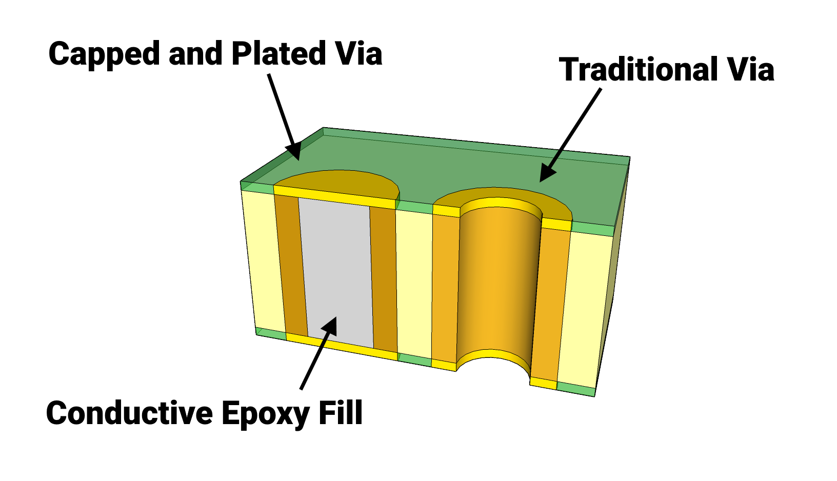
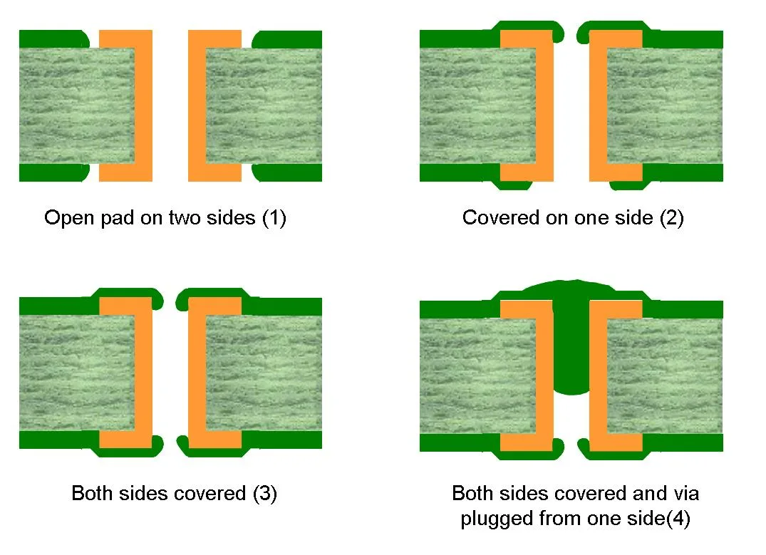
Several variations exist based on filling and covering methods. Unfilled vias use tenting, where solder mask covers the via to prevent solder wicking during assembly. Filled vias incorporate conductive or non-conductive epoxy to plug the hole, enhancing reliability under thermal stress. The choice depends on board thickness and component type. IPC-6012E outlines performance specs for such features in rigid printed boards, emphasizing plating thickness and hole quality. These principles ensure via-in-pad supports high-speed signals without impedance mismatches.
Fabrication tolerances play a critical role in via-in-pad success. Drill diameters typically match pad sizes closely, often around 0.3 mm for fine-pitch applications. Aspect ratios, the depth-to-diameter ratio, must stay manageable to avoid plating voids. Laser drilling enables smaller vias compared to mechanical methods, aiding density. Electrical testing verifies continuity post-fabrication. Understanding these mechanisms equips hobbyists to specify designs confidently.
Via-in-Pad Tutorial for Beginners: Step-by-Step Design Practices
Start your via-in-pad tutorial for beginners by planning the layer stackup early. Decide on via size based on the smallest pad in your electronic components, ensuring at least 0.1 mm annular ring around the via. Use design software to place vias centered under pads for BGAs or QFNs. Annular rings provide mechanical strength and prevent drill breakout. Set solder mask expansion to tent the via if unfilled, avoiding exposure. Always simulate thermal profiles to check heat dissipation.
Next, consider filling requirements for reliability. Conductive filling suits power or ground planes, distributing current evenly. Non-conductive fills work for signal vias, preventing shorts. IPC-A-600K defines acceptability criteria for filled vias, including void limits and surface flatness. Specify fill material in fabrication notes clearly. For hobbyists in PCB design for beginners, request plugged vias unless cost is a barrier.
Assembly compatibility is vital. Ensure via-in-pad does not cause solder voids under components. Use via caps or domes if open vias risk wicking flux. Test prototypes with X-ray inspection for hidden defects. Route signals away from vias to minimize crosstalk. These practices yield robust boards ready for electronic components.
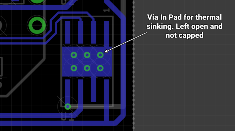
During routing, prioritize via-in-pad for escape routes from dense areas. Fan out pins systematically, using dog-bone shapes if vias slightly offset. Maintain consistent drill sizes across the board for uniform processing. Check DRC rules for minimum clearances. Document via types in a fab drawing. This structured approach simplifies what is via-in-pad implementation.
Common Challenges and Troubleshooting Tips
Hobbyists often face solderability issues with via-in-pad. Exposed vias can suck solder away from pads, weakening joints. Solution: tent or fill them properly. Warpage from mismatched thermal expansion affects multilayer boards with many vias. Select materials with similar CTE values. IPC-J-STD-001 provides guidelines for soldering acceptability, helping diagnose failures.
Another hurdle is fabrication yield. Undersized annular rings lead to rejects. Always add margins per design rules. Signal integrity degrades if vias introduce stubs. Use back-drilling for high-speed lines. For electronic hobbyists, start with 4-layer boards to practice. Troubleshooting builds intuition over time.
Conclusion
Via-in-pad transforms PCB design for beginners by enabling compact, efficient layouts for electronic components. From understanding what is via-in-pad basics to applying best practices, this technique empowers hobbyists to tackle denser projects. Key principles like filling and tenting ensure reliability, backed by industry standards. Challenges exist, but systematic troubleshooting resolves them. Experiment on prototypes to gain confidence. With these insights, your boards will perform better and fit more functionality.
FAQs
Q1: What is via-in-pad and when should beginners use it?
A1: Via-in-pad places a via directly under a surface mount pad, ideal for high-density PCB design for beginners. Use it with BGAs or fine-pitch electronic components to save space and improve routing. It matters for prototypes needing compact footprints. Always check fab capabilities first. This via-in-pad basics approach enhances hobby projects without complexity.
Q2: How does via-in-pad affect assembly of electronic components?
A2: In via-in-pad tutorial for beginners, tenting prevents solder wicking, ensuring strong joints for electronic components. Filled vias provide flat surfaces for reflow soldering. Poor implementation causes voids, so specify plugging. Test with thermal profiling. Reliable assembly follows standards for hobbyist success.
Q3: What are common mistakes in via-in-pad basics for PCB design?
A3: Beginners overlook annular ring sizes, leading to fab failures in via-in-pad basics. Insufficient tenting exposes vias, risking shorts. Ignore stackup effects on aspect ratios. Solution: use DRC checks and consult fab guides. Proper planning avoids rework in PCB design for beginners.
Q4: Can via-in-pad improve thermal performance in hobby projects?
A4: Yes, filled via-in-pad conducts heat from electronic components to inner planes effectively. Multiple vias under hot chips dissipate power better than traces. Consider fill material conductivity. This boosts reliability in dense layouts. Hobbyists benefit from simple thermal vias.
References
IPC-6012E — Qualification and Performance Specification for Rigid Printed Boards. IPC, 2017
IPC-A-600K — Acceptability of Printed Boards. IPC, 2020
IPC-J-STD-001H — Requirements for Soldered Electrical and Electronic Assemblies. IPC, 2018





