ALLPCB


What Is Via Aspect Ratio and Why It Matters
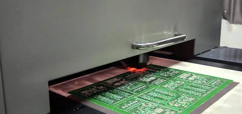
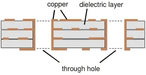
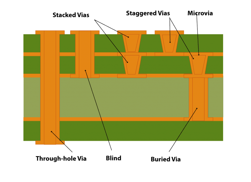
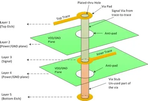
Via aspect ratio quantifies the physical proportions of a plated through-hole or blind via. A typical value is expressed as depth divided by diameter, with higher ratios indicating narrower or deeper holes relative to their width. In high-speed designs, this ratio affects the via’s electrical behavior because longer current paths increase series inductance while the barrel and pads add shunt capacitance. When the aspect ratio exceeds recommended limits for a given stack-up, the via can create a noticeable impedance mismatch that reflects energy back toward the driver. These reflections combine with via stub effects, where unused via segments act as open stubs and resonate at frequencies determined by their length. The result is increased insertion loss, jitter, and potential violation of timing budgets in protocols such as PCIe or Ethernet. Industry standards such as IPC-6012E establish baseline requirements for via formation and plating that indirectly support reliable electrical performance when aspect ratios remain within practical fabrication limits.
Technical Principles and Mechanisms
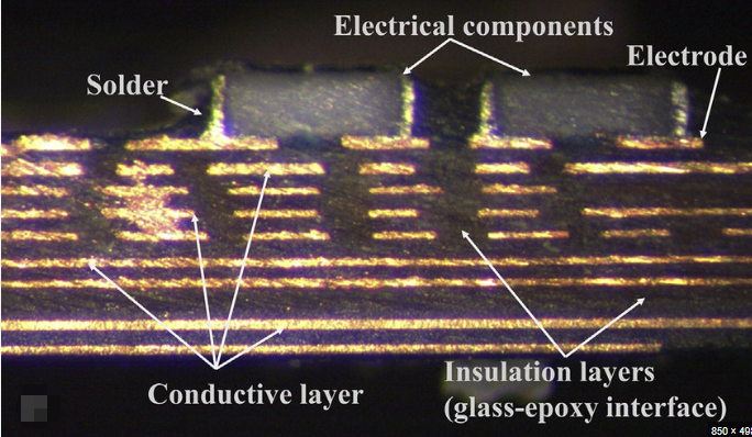
Signal propagation through a via can be modeled as a short transmission line segment whose characteristic impedance depends on the surrounding dielectric, the barrel diameter, and the pad geometry. A high aspect ratio via lengthens this segment, raising its inductive reactance at higher frequencies and lowering the effective impedance relative to the target board impedance, often 50 Ω or 100 Ω differential. The abrupt change in geometry at the via entry and exit points produces a capacitive discontinuity that further distorts the signal waveform. Via stub effects become pronounced when the via continues beyond the signal layer into unused inner layers; the stub length determines the quarter-wave resonance frequency that can fall within the signal bandwidth. Reflections caused by these discontinuities add vectorially at the receiver, closing the eye diagram and elevating bit-error rates. In addition, the increased surface area of a high-aspect-ratio barrel raises conductor losses, especially when skin effect confines current to the plating surface. PCB impedance control strategies must therefore account for via parasitics alongside trace width and dielectric thickness to keep the overall channel response within specification.
Practical Solutions and Best Practices
Design teams reduce via-related signal integrity issues by selecting the lowest practical aspect ratio consistent with the board thickness and layer count. This often means using larger via diameters or thinner cores when routing density permits. Back-drilling, or controlled-depth drilling that removes the unused via stub after plating, shortens the effective stub length and shifts its resonant frequency outside the operating band. Via-in-pad constructions with filled and capped vias allow signals to transition layers with minimal stub while maintaining a continuous return path. When back-drilling is not feasible, designers may route critical nets on outer layers or employ blind and buried vias that inherently limit stub length. Simulation of the full channel, including extracted via models, verifies that reflections remain below acceptable thresholds before committing to fabrication. Layout guidelines typically recommend keeping via aspect ratios below 10:1 for high-speed signals, although the exact limit depends on frequency, stack-up, and required margin. Adherence to IPC-A-600K acceptability criteria ensures that fabricated vias meet the geometric tolerances assumed during simulation.
Additional Design Considerations for Signal Integrity
Engineers also evaluate the cumulative effect of multiple vias along a net. Each via contributes a small reflection, and their spacing can create periodic discontinuities that produce notches in the frequency response. Differential pairs require matched via pairs with symmetric return paths to preserve common-mode rejection. Placement of stitching vias or ground vias adjacent to signal vias helps maintain a low-inductance return path and reduces radiation. Thermal relief connections around vias, while useful for assembly, can increase inductance and should be avoided on high-speed nets. Documentation of via parameters in the fabrication drawing, including finished hole size, plating thickness, and back-drill depth when applicable, enables the manufacturer to meet the electrical intent of the design.
Conclusion
Via aspect ratio is a fundamental geometric parameter that influences reflections, losses, and overall signal integrity in high-speed PCBs. By understanding the mechanisms of impedance discontinuity and via stub effects, designers can apply targeted mitigation techniques such as back-drilling and optimized via sizing. These choices, combined with thorough simulation and adherence to established industry standards, help ensure that boards meet performance requirements without costly respins. Early attention to via geometry during stack-up definition and layout yields measurable improvements in eye opening and reduces the risk of field failures related to interconnect integrity.
FAQs
Q1: How does via aspect ratio affect signal reflections in high-speed designs?
A1: A higher via aspect ratio increases the inductive and capacitive parasitics of the via barrel, creating larger impedance mismatches that reflect portions of the incident signal. These reflections add to via stub effects and degrade timing margins. Maintaining lower aspect ratios or employing back-drilling helps minimize such discontinuities while supporting PCB impedance control targets.
Q2: What role does via aspect ratio play in PCB impedance control?
A2: Via aspect ratio determines the length and diameter of the conductive path through the board, directly influencing the via’s contribution to the overall transmission-line impedance. When the ratio is too high, the via deviates from the target impedance of the surrounding traces, introducing reflections. Careful selection of diameter and depth during stack-up planning keeps via parasitics within acceptable limits for the intended data rate.
Q3: Can via stub effects be eliminated by adjusting via aspect ratio alone?
A3: Reducing via aspect ratio shortens the total via length and can lessen stub impact, yet complete elimination usually requires additional techniques such as back-drilling or blind-via structures. Aspect ratio optimization works best when combined with these methods to shift or remove resonant frequencies outside the signal bandwidth.
Q4: What industry standards guide via formation for signal integrity applications?
A4: Standards such as IPC-6012E define qualification requirements for rigid printed boards, including via plating and dimensional tolerances that support reliable electrical performance. IPC-A-600K provides visual and dimensional acceptance criteria that help ensure fabricated vias meet the geometric assumptions used in signal-integrity simulations.
References
IPC-6012E — Qualification and Performance Specification for Rigid Printed Boards. IPC, 2017
IPC-A-600K — Acceptability of Printed Boards. IPC, 2020
IPC-2221B — Generic Standard on Printed Board Design. IPC, 2012