 ALLPCB


Why White Silkscreen Matters in LED Applications
LED PCBs require careful management of light paths to achieve desired illumination levels. Traditional green or black solder masks absorb a portion of the emitted light, reducing effective output. White silkscreen addresses this by providing a high-reflectivity surface that bounces light back into the intended direction. Designers incorporate it in applications such as panel lighting, automotive fixtures, and architectural installations where uniform brightness and clean aesthetics are priorities. The choice influences both thermal management and long-term visual consistency of the finished assembly.
Technical Principles of Reflective Silkscreen
The silkscreen layer consists of a polymer-based ink formulated with reflective pigments. When light from surface-mount LEDs strikes the white surface, a significant fraction reflects rather than being lost to absorption. This mechanism increases the amount of usable light exiting the fixture. Reflectivity depends on ink formulation, application thickness, and surface smoothness achieved during curing. In LED PCB design, engineers evaluate the interaction between the silkscreen and the solder mask to avoid unintended shadowing or color shifts over time. The result is measurable improvement in luminous efficacy for the overall board assembly.
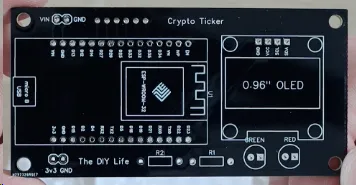
Surface preparation before silkscreen application affects final performance. Proper cleaning removes contaminants that could reduce adhesion or create uneven reflectivity. Curing parameters must align with the ink chemistry to produce a stable, non-yellowing finish under prolonged exposure to LED operating temperatures. Engineers often model light distribution using ray-tracing simulations that incorporate the silkscreen optical properties. These models help predict efficiency gains before physical prototypes are built.
Design Considerations for LED PCB Layout
Placement of white silkscreen requires coordination with copper traces, thermal vias, and component footprints. The layer typically covers non-functional areas while leaving solder pads and test points exposed. Designers maintain adequate clearance around high-power LEDs to prevent interference with heat dissipation paths. In dense layouts, selective application prevents the silkscreen from bridging fine-pitch features that could compromise electrical isolation. This structured approach ensures both optical benefits and manufacturing yield remain high.
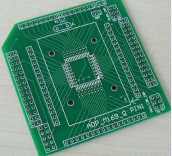
Material compatibility between the silkscreen ink and the underlying laminate or solder mask must be verified. Thermal expansion differences can lead to cracking or delamination if coefficients are mismatched. Engineers reference established qualification procedures to confirm long-term reliability under temperature cycling. Aesthetic goals also influence decisions, such as achieving uniform color across large panels or matching surrounding housing finishes.
Manufacturing and Quality Aspects
Application of white silkscreen follows standard screen-printing or direct imaging processes used in PCB fabrication. Thickness control is critical because excessive buildup can affect component seating while insufficient coverage reduces reflectivity. Post-print inspection verifies coverage uniformity and absence of defects that could scatter light unpredictably. Quality teams evaluate adhesion through standardized test methods to ensure the layer withstands subsequent assembly steps and field conditions.
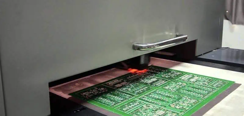
Industry standards guide acceptable quality levels for the finished board. IPC-A-600K outlines visual and dimensional criteria that apply to silkscreen features. IPC-6012E provides qualification requirements for rigid boards that encompass surface finish characteristics relevant to optical performance. These references help maintain consistency across production lots without introducing proprietary process details.
Conclusion
White silkscreen offers a practical method to enhance light output and improve the appearance of LED PCBs. Its reflective characteristics support efficiency gains when integrated thoughtfully into the design. Careful attention to layout, material selection, and process control ensures reliable results that meet engineering and quality expectations. Engineers who apply these principles can achieve balanced performance in demanding lighting applications.
FAQs
Q1: How does white silkscreen improve LED efficiency?
A1: White silkscreen reflects light that would otherwise be absorbed by darker board surfaces. This increases the amount of usable illumination from each LED without requiring additional power. Proper application in LED PCB design contributes to higher overall luminous efficacy while maintaining standard thermal performance.
Q2: What factors affect the reflectivity of silkscreen for LED boards?
A2: Reflectivity depends on ink formulation, applied thickness, and surface finish quality after curing. Designers consider compatibility with the solder mask and laminate to avoid performance degradation. Consistent process control during manufacturing supports repeatable optical results across production.
Q3: When should white silkscreen be used in LED PCB design?
A3: White silkscreen suits applications where maximizing light output and achieving clean aesthetics are priorities. It works well in panel, strip, and module formats for commercial and industrial lighting. Engineers evaluate trade-offs with cost and process complexity before specifying the layer.
Q4: Does white silkscreen impact long-term reliability of LED boards?
A4: When applied according to established quality criteria, white silkscreen maintains adhesion and optical properties through typical operating conditions. Standards such as those in IPC-6012E address relevant board qualification aspects. Proper material selection and process validation minimize risks of discoloration or delamination over time.
IPC-A-600K — Acceptability of Printed Boards. IPC, 2020
IPC-6012E — Qualification and Performance Specification for Rigid Printed Boards. IPC, 2017





