 ALLPCB


The Importance of Annular Rings in Plated Through-Hole Reliability
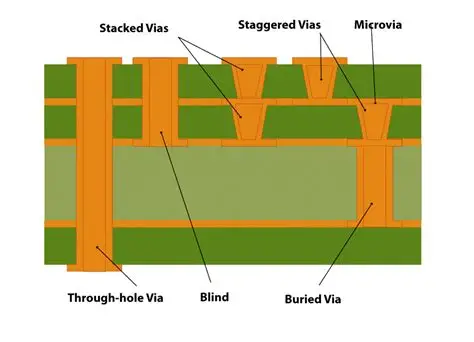
Plated through-holes, or PTHs, serve as critical vertical interconnections in multilayer printed circuit boards. These holes allow electrical signals and power to pass between layers while providing mechanical support for component leads. The annular ring, the copper area surrounding each PTH, directly influences the long-term reliability of these connections. For electrical engineers working on high-performance designs, understanding annular ring behavior helps prevent failures that arise from thermal cycling, mechanical stress, or manufacturing variations. Proper attention to PTH annular ring size supports consistent performance across demanding applications.
What Is an Annular Ring and Why It Matters
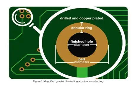
An annular ring consists of the copper land that remains around a drilled and plated hole after fabrication. Its width is determined by the difference between the pad diameter and the finished hole diameter. In PTH structures, this ring ensures both electrical continuity through the plating and mechanical integrity under load. Insufficient annular ring width increases the risk of annular ring breakout, where the copper connection is partially or fully lost due to misalignment or over-etching. Such breakout compromises PCB reliability by creating high-resistance paths or open circuits over time. Industry standards define acceptance criteria to balance design density with manufacturing capability.
Technical Principles of Annular Ring Formation and Failure Mechanisms
During PCB fabrication, the annular ring forms through a sequence of drilling, plating, and etching steps. Registration accuracy between layers, drill wander, and etch factors all affect the final ring width. When tolerances accumulate, the copper may not fully surround the hole, resulting in breakout on one or more sides. Electrically, a reduced or missing ring increases current density at the remaining contact points, raising the potential for localized heating. Mechanically, the ring distributes stress from component insertion, vibration, or thermal expansion mismatches between copper and dielectric materials. Under repeated thermal cycles, inadequate annular ring width can accelerate barrel cracking or delamination at the hole wall. These mechanisms explain why minimum annular ring requirements exist to maintain both conductivity and structural stability throughout the product life cycle.
Annular Ring Calculation and Design Considerations
Annular ring calculation begins with the nominal pad size minus the finished hole diameter, divided by two to obtain the radial width. Designers must account for manufacturing allowances such as drill tolerance, etch undercut, and layer-to-layer registration when setting the minimum annular ring. IPC-2221 provides guidance on these allowances to achieve target producibility levels. Increasing the pad diameter improves the margin against breakout but consumes routing space on dense boards. Conversely, aggressive minimization of PTH annular ring size raises the probability of defects during volume production. Engineers therefore evaluate trade-offs between board density, assembly requirements, and expected environmental stresses when specifying annular ring dimensions.
Best Practices for Ensuring PTH Reliability
Design teams achieve reliable PTH performance by applying conservative annular ring targets early in the layout phase and communicating class requirements clearly to fabrication partners. Following the acceptance criteria outlined in IPC-6012E helps align design intent with manufacturing capability. During prototyping, microsection analysis verifies actual annular ring widths against specifications and identifies any systematic registration issues. In production, statistical process control on drilling and imaging steps maintains consistency. When space constraints force smaller rings, techniques such as teardrop pad shapes or optimized via placement can improve the effective connection area without violating minimum annular ring rules. Regular design rule checks that incorporate fabrication tolerances reduce the incidence of annular ring breakout and support higher overall PCB reliability.
Conclusion
Annular rings form the foundation of reliable plated through-hole interconnections. Their size directly affects electrical performance, mechanical strength, and resistance to environmental stresses. By applying structured calculation methods, respecting industry-defined acceptance limits, and incorporating manufacturing realities into the design process, engineers can minimize breakout risks and extend product life. Consistent attention to these details translates into fewer field failures and more predictable board behavior across production volumes.
FAQs
Q1: What factors determine the minimum annular ring required for a PTH?
A1: The minimum annular ring depends on the performance class of the board, layer registration tolerances, drill accuracy, and etch characteristics. Electrical engineers reference IPC-6012E to establish class-specific limits that balance density with reliability. Adequate margin above the minimum helps accommodate process variations and maintains PCB reliability under thermal and mechanical loads.
Q2: How does annular ring breakout affect long-term PCB reliability?
A2: Annular ring breakout reduces the contact area between the hole plating and the copper land, increasing resistance and current density. Over time, this condition can lead to intermittent connections or complete opens, especially under thermal cycling or vibration. Standards such as IPC-A-600K define the maximum acceptable breakout angles to prevent these reliability issues.
Q3: What is the role of annular ring calculation in the PCB design workflow?
A3: Annular ring calculation incorporates finished hole size, pad diameter, and fabrication allowances to predict the final copper width. Performing this calculation early allows designers to adjust pad sizes or via locations before layout completion. The process supports compliance with minimum annular ring requirements and reduces the likelihood of costly redesigns later in the project.
Q4: Why is PTH annular ring size particularly important in high-reliability applications?
A4: High-reliability designs experience greater thermal and mechanical stresses that amplify any weakness at the PTH interface. A properly sized annular ring distributes stress evenly and maintains low-resistance paths throughout the product lifetime. Adherence to established standards ensures consistent performance even when boards operate in demanding environments.
References
IPC-6012E — Qualification and Performance Specification for Rigid Printed Boards. IPC, 2017
IPC-A-600K — Acceptability of Printed Boards. IPC, 2020
IPC-2221B — Generic Standard on Printed Board Design. IPC, 2012





