 ALLPCB


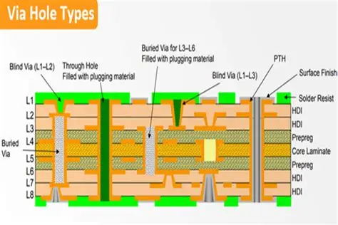
In printed circuit board design, vias serve as the electrical bridges between layers, and their performance depends heavily on the quality of the copper plating inside them. Engineers must balance via geometry with plating processes to maintain consistent conductivity and mechanical strength across the board. Poor control over these elements can lead to intermittent connections or outright failures under thermal or mechanical stress. The relationship between via aspect ratio and copper plating thickness directly influences signal integrity and long-term reliability in multilayer designs. Understanding these factors helps design teams create boards that meet demanding performance requirements without unnecessary complexity.
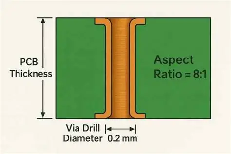
What Is Via Aspect Ratio and Why It Matters
Via aspect ratio is defined as the ratio of the via depth to its diameter, a key parameter that governs how uniformly copper can be deposited during plating. Higher ratios create deeper, narrower holes that challenge the plating solution’s ability to reach all surfaces evenly. Copper plating thickness inside the via must remain consistent to provide adequate current-carrying capacity and to withstand repeated thermal cycling. In multilayer boards, variations in plating can create weak points that affect both electrical performance and mechanical integrity. Industry standards such as IPC-6012 establish acceptance criteria for these characteristics to ensure boards perform as intended in their final assemblies. Proper management of aspect ratio and plating supports the overall goal of producing reliable interconnections that maintain continuity throughout the product’s life.
Technical Principles of the Via Plating Process
The via plating process typically begins with electroless plating, which deposits a thin, uniform seed layer of copper on the hole walls without requiring an external electrical current. This initial layer provides the conductive path needed for subsequent electrolytic plating, where thicker copper is built up through an applied current. Electroless plating excels at covering complex surfaces but deposits copper at a slower rate and with less thickness control compared to electrolytic methods. In high aspect ratio vias, the plating solution experiences reduced agitation and ion transport deep within the hole, leading to thinner deposits near the center and potential voids if process parameters are not optimized. Copper plating thickness must be monitored at multiple points along the via wall to verify uniformity, as uneven distribution increases resistance and creates stress concentrations. These mechanisms highlight why aspect ratio limits are considered early in the design phase to avoid downstream manufacturing difficulties.
High Aspect Ratio Plating Challenges
High aspect ratio plating challenges arise primarily from limited mass transport of copper ions into narrow, deep vias, resulting in non-uniform thickness along the barrel. The center of the via often receives less copper than the entrance and exit areas, creating a barrel-shaped profile that reduces effective conductivity. Electroless plating helps initiate coverage but may not compensate fully for these geometric constraints during the build-up phase. Thermal expansion differences between the copper and the surrounding dielectric can exacerbate stress at thinner sections, potentially causing cracks over time. Design teams address these issues by evaluating via diameter relative to board thickness and selecting plating chemistries with improved throwing power. Process controls such as optimized agitation, temperature, and current density further mitigate risks associated with elevated aspect ratios.
Practical Solutions and Best Practices
Designers can reduce high aspect ratio plating challenges by specifying via diameters that maintain moderate aspect ratios suited to the board thickness and expected current loads. Collaboration between design and manufacturing teams ensures that copper plating thickness targets align with both electrical requirements and process capabilities. Sequential build-up or filled vias may be considered when standard through-hole plating proves insufficient for very high ratios. Regular verification of plating uniformity through cross-section analysis supports consistent quality across production lots. Adherence to established guidelines, such as those in IPC-A-600, provides clear acceptance criteria for plated vias and helps identify deviations early. These practices promote reliable connections while keeping the overall board fabrication process efficient and repeatable.
Conclusion
Via aspect ratio and copper plating thickness remain fundamental considerations in achieving dependable interlayer connections in printed circuit boards. By understanding the plating process, recognizing the limitations imposed by high aspect ratios, and applying structured design and process controls, engineers can minimize risks of electrical discontinuity or mechanical failure. Consistent application of industry-accepted practices supports the production of boards that perform reliably under real-world conditions.
FAQs
Q1: What factors influence copper plating thickness in vias?
A1: Copper plating thickness in vias depends on the via aspect ratio, the sequence of electroless and electrolytic plating steps, and process parameters such as solution chemistry and current density. Maintaining uniform thickness ensures adequate conductivity and mechanical strength throughout the via barrel.
Q2: How does the via plating process address high aspect ratio plating challenges?
A2: The via plating process uses an initial electroless copper layer to seed the hole walls, followed by electrolytic plating to build thickness. Improved solution agitation and chemistry formulations help overcome ion transport limitations in high aspect ratio vias, promoting more even deposition along the entire depth.
Q3: Why is electroless plating important before electrolytic copper deposition?
A3: Electroless plating provides a thin, conductive seed layer on non-conductive surfaces inside the via without requiring electrical contact. This layer enables the subsequent electrolytic process to deposit thicker copper uniformly, which is essential for achieving reliable connections in multilayer boards.
Q4: What design considerations help manage via aspect ratio for reliable plating?
A4: Designers evaluate board thickness against via diameter early in the layout phase to keep aspect ratios within practical limits for uniform plating. Selecting appropriate via sizes and considering alternative structures when needed supports consistent copper plating thickness and long-term connection reliability.
References
IPC-6012E — Qualification and Performance Specification for Rigid Printed Boards. IPC, 2017
IPC-A-600K — Acceptability of Printed Boards. IPC, 2020


