ALLPCB


When it comes to mass-producing printed circuit boards, panelization plays a critical role in manufacturing efficiency, cost control, and product quality. Among the various panelization techniques available, V-Cut (V-Scoring) and Tab-Routing are the two most widely used methods. Each method has its own set of advantages and limitations, and choosing the right one can significantly impact the final outcome of your project. In this article, we’ll explore the key differences between V-Cut and Tab-Routing, along with their respective pros and cons, to help you make an informed decision.
What Is PCB Panelization?
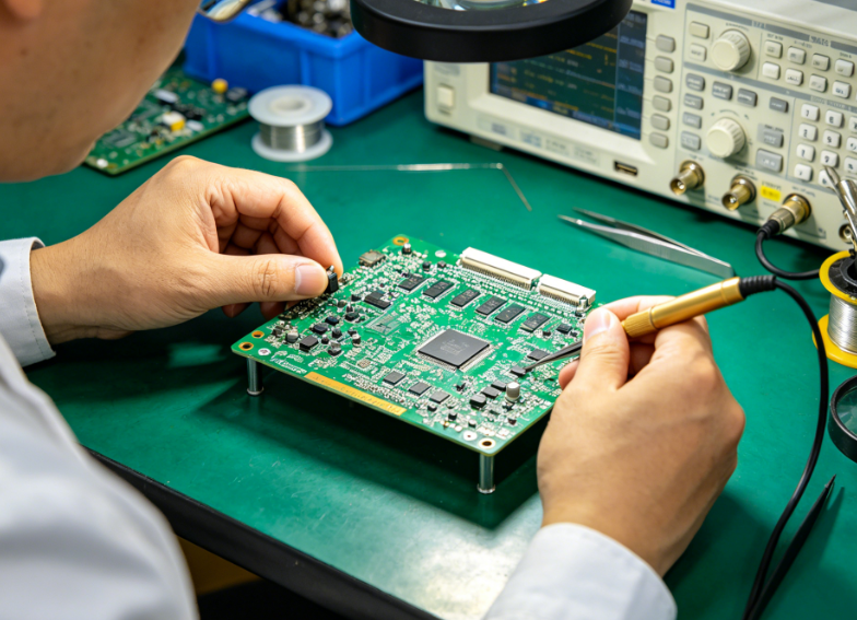
PCB panelization refers to the process of grouping multiple individual PCBs into a single panel during manufacturing. This enables automated assembly, simplifies handling, and reduces production costs. After PCB assembly, the individual boards are separated (depanelized) using a mechanical method based on the chosen panelization strategy.
What Is V-Cut (V-Scoring)?
V-Cut involves cutting V-shaped grooves along the top and bottom surfaces of a PCB panel, leaving a thin layer of material in the middle. These grooves act as break lines, making it easy to snap individual boards apart after assembly. The cuts are usually straight lines, either vertical or horizontal, and the boards are separated by applying pressure along the score lines.
Pros of V-Cut:
- Higher Panel Density: Since V-Cut doesn’t require space for tabs, boards can be placed closer together, optimizing the use of panel area.
- Lower Cost: It is generally more cost-effective due to simpler tooling and faster cutting processes.
- Faster Depanelization: Boards can be separated quickly with minimal mechanical effort.
- Ideal for Straight-Edged Boards: Best suited for rectangular or square boards with straight edges.
Cons of V-Cut:
- Limited to Straight Lines: Can’t be used for irregular or curved board shapes.
- Mechanical Stress: Breaking the boards apart can cause stress along the edges, potentially damaging components placed too close to the break line.
- Rough Edges: The break line may leave slightly jagged or uneven edges, requiring post-processing in sensitive applications.
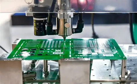
What Is Tab-Routing?
Tab-Routing involves creating small tabs between individual PCBs within a panel. These tabs typically include breakaway holes (mouse bites) that make the separation process easier. A routing bit cuts around the PCB outline, and the tabs hold the boards in place until final separation.
Pros of Tab-Routing:
- Supports Complex Shapes: Suitable for non-rectangular and irregular PCB outlines.
- Less Mechanical Stress: Offers a cleaner and more controlled break, reducing the risk of component or board damage.
- Smooth Edges: Post-depanelization edges are usually cleaner, which is ideal for high-precision applications.
Cons of Tab-Routing:
-
Wastes Panel Space: Tabs and routing paths require additional clearance, reducing panel utilization.
-
Higher Cost: More complex tooling and longer routing times increase the custom PCB cost.
- Slower Depanelization: Requires manual or semi-automated tools (like depaneling routers or punching machines) to remove the boards, which takes more time.
Choosing the Right Method
Choosing between V-Cut and Tab-Routing depends on your specific project requirements:
- Board Shape: Use V-Cut for simple, straight-edged designs; choose Tab-Routing for complex or irregular shapes.
- Component Placement: Avoid placing components too close to V-Cut lines. Tab-Routing provides better protection in densely populated PCBs.
- Production Volume: V-Cut is often favored in high-volume runs due to its speed and cost-effectiveness.
- Edge Quality Needs: If aesthetics and edge smoothness are critical, Tab-Routing is the better choice.
- Panel Efficiency: For maximum board density, V-Cut offers better panel utilization.
Hybrid Approach
In some cases, a hybrid approach that combines both V-Cut and Tab-Routing may be used to optimize manufacturing. For example, straight edges may use V-Cut while curved areas are supported by Tab-Routing. This provides a balance between cost, edge quality, and shape flexibility.
Final Thoughts
Both V-Cut and Tab-Routing are reliable panelization techniques, each with its own strengths and weaknesses. Understanding your product's mechanical, aesthetic, and cost requirements will help you choose the best method. By collaborating closely with your PCB manufacturer, you can design a panelization strategy that ensures smooth production and high-quality results.