ALLPCB


Introduction
Aspect ratio plays a central role in PCB stack-up design because it directly connects board thickness to the diameter of drilled vias. Engineers must balance these dimensions to ensure reliable plating, mechanical stability, and electrical performance across multilayer constructions. When aspect ratio exceeds practical limits, drilling and plating processes become more challenging, which can affect overall yield during PCB manufacturing. Proper consideration of aspect ratio early in the design phase helps maintain consistent quality while meeting the requirements of modern high-density interconnect boards. This relationship between via geometry and stack-up thickness influences decisions on material selection and layer count from the outset.
What Is PCB Aspect Ratio and Why It Matters
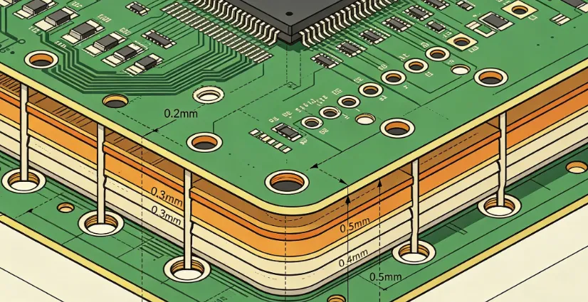
PCB aspect ratio is defined as the ratio of the finished board thickness to the diameter of the drilled via hole. This value determines how deeply a drill must penetrate relative to its width, which directly affects the feasibility of via drilling in multilayer stack-ups. In PCB manufacturing, higher aspect ratios require more precise control over drill speed, feed rate, and coolant delivery to avoid issues such as hole wall roughness or drill breakage. Designers working with thicker stack-ups often select larger via diameters to keep the aspect ratio within acceptable bounds, thereby supporting reliable copper plating inside the holes. The choice of aspect ratio also influences thermal expansion behavior and mechanical stress distribution across the board during assembly and operation. Understanding this parameter early allows teams to align stack-up specifications with downstream manufacturing capabilities without unnecessary redesign iterations.
Technical Principles and Mechanisms
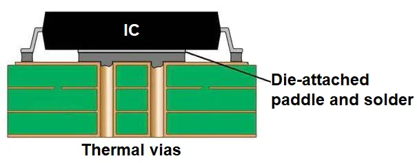
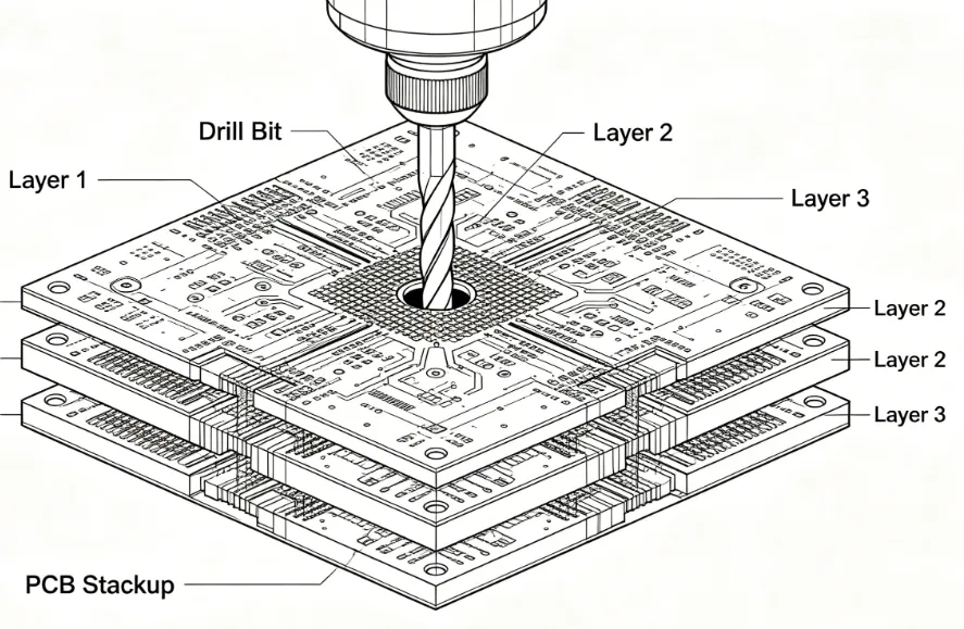
The mechanics of via formation in a PCB stack-up begin with mechanical or laser drilling through the laminated layers. As board thickness increases relative to hole diameter, the aspect ratio rises and the plating chemistry must travel farther into narrow channels to deposit uniform copper. This process becomes sensitive to solution flow dynamics and current distribution, which can result in thinner plating at the via center if the ratio grows too large. Thermal stresses during reflow or operational cycling further test the integrity of high-aspect-ratio vias because the copper barrel must accommodate differential expansion between the board material and the metal deposit. Industry standards such as IPC-2221 provide design guidelines that help engineers evaluate these interactions when defining stack-up parameters. Maintaining control over aspect ratio therefore supports both electrical continuity and long-term reliability in finished assemblies.
Related Reading: Calculating PCB Aspect Ratio: A Step by Step Guide for Beginners
Practical Solutions and Best Practices
Engineers can manage aspect ratio by selecting via diameters that scale appropriately with planned board thickness during the initial stack-up definition. For thicker constructions, incorporating multiple smaller vias in parallel or using filled vias can distribute current and reduce individual aspect ratios while preserving routing density. Collaboration between design and manufacturing teams early in the project helps identify the maximum aspect ratio that the chosen fabrication process can reliably achieve. Simulation tools that model plating thickness distribution allow verification of proposed via geometries before committing to prototypes. Regular review of stack-up drawings against IPC-6012 requirements ensures that aspect ratio decisions remain aligned with qualification criteria for rigid printed boards. These steps collectively reduce the risk of plating voids or mechanical failures that could arise from overly aggressive aspect ratios.
Related Reading: Demystifying PCB Aspect Ratio: A Comprehensive Guide for Optimal Designs
Manufacturing and Quality Considerations
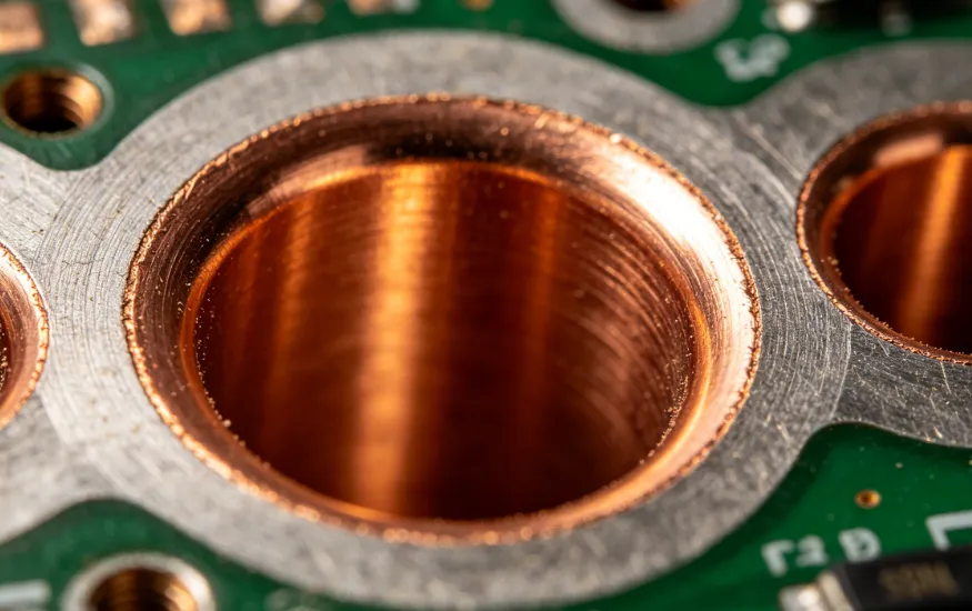
During PCB manufacturing, drill bit selection and spindle speed must be optimized for the target aspect ratio to produce clean hole walls that accept uniform plating. Post-drilling inspection techniques, including cross-section analysis, confirm that copper deposition meets thickness specifications even in high-ratio vias. Quality control procedures outlined in IPC-A-600 help inspectors evaluate hole wall quality and plating coverage without relying solely on electrical testing. When aspect ratios approach the upper limits of a given process, additional steps such as pulse plating or vacuum-assisted filling may be introduced to improve deposit uniformity. These manufacturing adjustments directly support the reliability targets established during the stack-up design phase.
Conclusion
Aspect ratio serves as a fundamental link between PCB thickness, via drilling, and overall stack-up performance. By addressing this parameter through structured design practices and adherence to recognized standards, engineers can achieve reliable multilayer boards that meet both functional and manufacturing requirements. Consistent attention to aspect ratio throughout the development cycle supports higher yields and reduces the likelihood of field failures related to via integrity.
FAQs
Q1: What is the recommended PCB aspect ratio for reliable via drilling?
A1: A typical target for standard PCB manufacturing keeps the aspect ratio at or below 10:1 to ensure uniform plating and mechanical stability. Designers evaluate board thickness and via diameter together during stack-up planning to stay within this range. Following guidelines from IPC-2221 helps confirm that the chosen ratio supports both drilling and plating processes without introducing defects.
Q2: How does PCB thickness influence aspect ratio in multilayer stack-ups?
A2: Greater PCB thickness increases the aspect ratio for any given via diameter, which can complicate via drilling and copper deposition. Engineers adjust via sizes or layer counts early in design to maintain manufacturability. This relationship directly affects decisions on material selection and via placement within the stack-up.
Q3: Why is aspect ratio important during PCB manufacturing?
A3: Aspect ratio determines the difficulty of achieving consistent plating inside drilled holes and influences overall board reliability. Manufacturing teams use it to set process parameters for drilling speed and plating chemistry. Proper management of this value helps meet acceptance criteria defined in IPC-6012 for rigid printed boards.
Q4: Can aspect ratio affect signal integrity in high-speed PCB designs?
A4: Higher aspect ratios can introduce variations in via inductance and capacitance that impact signal transmission. Designers therefore balance aspect ratio with stack-up impedance targets to preserve performance. Early simulation of via geometry within the stack-up helps identify and mitigate these effects before fabrication.