 ALLPCB


Introduction
Metal-backed PCBs provide reliable thermal management in demanding electronic systems. Engineers select these boards when standard FR-4 constructions cannot dissipate heat effectively from high-power components. The metal substrate, typically aluminum or copper, conducts heat away from active devices while maintaining electrical isolation through a thin dielectric layer. This construction supports higher current densities and longer operating life in compact assemblies. Designers working with power electronics, LED arrays, and motor drives frequently specify metal-backed PCBs to meet strict thermal budgets without adding bulky heatsinks.
What Is a Metal-Backed PCB and Why It Matters
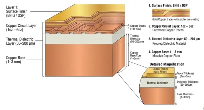
A metal-backed PCB consists of a copper circuit layer bonded to a metal base plate through a thermally conductive dielectric. The base plate, most often aluminum or copper, acts as both a mechanical support and a heat spreader. In contrast to conventional rigid boards, the metal layer lowers thermal resistance from component junction to ambient air. This property becomes critical in applications where junction temperatures must remain below 125 degrees Celsius under continuous load. Procurement teams and design engineers choose aluminum backed PCB options for cost-sensitive projects and copper backed PCB constructions when maximum thermal conductivity is required. Industry adoption continues to grow in automotive, industrial automation, and renewable energy sectors because these boards reduce system size and improve reliability.
Technical Principles of Heat Transfer in Metal-Backed PCBs
Heat generated by power semiconductors flows through the dielectric layer into the metal base, then spreads laterally before transferring to the enclosure or heatsink. Thermal conductivity of the dielectric, typically 1 to 3 watts per meter-kelvin, determines the overall performance more than the metal thickness itself. Copper backed PCB constructions achieve lower thermal resistance than aluminum versions because copper conducts heat roughly twice as efficiently. Engineers model this behavior using finite element analysis to predict hot-spot locations and required copper thickness. The dielectric must also withstand voltage stresses without breakdown, so material selection balances thermal performance against electrical insulation requirements. Warpage during reflow soldering remains a key concern because the coefficient of thermal expansion mismatch between copper and aluminum can induce mechanical stress.
Design Considerations for Metal-Backed PCBs
Designers following a structured metal-backed PCB design guide begin by calculating the required thermal resistance from component junction to case. They then select dielectric thickness and thermal conductivity to meet that target while satisfying voltage isolation needs. Thermal vias placed directly under heat-generating devices further reduce resistance by providing low-impedance paths to the metal core. Trace widths and copper weights are increased in high-current areas to limit temperature rise according to standard current-carrying capacity charts. Component placement avoids clustering high-power devices in one region to prevent localized overheating. Edge clearance and mounting hole locations must account for the rigid metal base, which does not flex like standard laminates.
Related Reading: Copper vs. Aluminum MCPCB: Choosing the Right Metal Core for Your PCB
Metal-Backed PCB Manufacturing Process
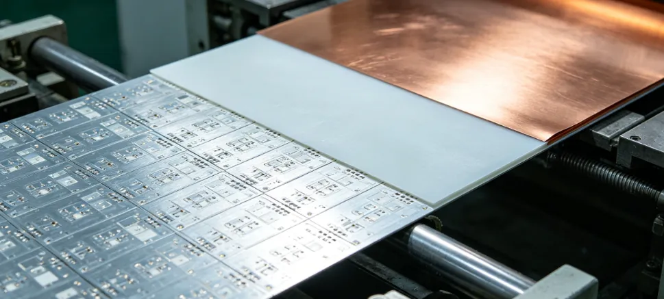
The manufacturing process for metal-backed PCBs follows established sequences but requires specialized handling of the thick metal substrate. Sophia Wang notes that panels are first drilled or routed to create mounting features and via holes before the dielectric and copper foil are laminated under controlled pressure and temperature. Circuit patterns are then formed through standard photolithography and etching steps. Quality control teams verify dielectric thickness and thermal conductivity on every lot to maintain consistency. Surface finishes such as HASL or ENIG are applied after etching, with care taken to avoid damaging the exposed metal base edges. Final routing separates individual boards while preserving flatness to within 0.15 millimeters per 100 millimeters, as required for reliable assembly.
Practical Assembly and Application Guidance
Grace Li emphasizes that assembly processes for metal-backed PCBs differ from standard boards primarily in reflow profiling and handling. The high thermal mass of the metal core requires longer soak times and slightly higher peak temperatures to ensure proper solder joint formation. SMT stencils are designed with larger apertures in thermal pad areas to deposit adequate solder volume. Post-assembly inspection focuses on voiding under large thermal pads, which can be reduced by optimizing paste volume and reflow atmosphere. In field applications, aluminum backed PCB solutions appear in LED lighting modules where cost and weight matter, while copper backed PCB versions serve high-reliability power converters in electric vehicles and industrial drives. Both types support direct attachment to heatsinks or chassis walls, eliminating the need for separate thermal interface materials in some designs.
Troubleshooting Common Issues in Metal-Backed PCB Designs
Thermal performance shortfalls often trace back to insufficient via density or dielectric material selection. Engineers measure actual board temperatures with infrared cameras or embedded thermocouples during prototype validation. Warpage exceeding 0.5 percent can cause component cracking or poor solder joint quality, so process controls during lamination and cooling are essential. Electrical isolation failures usually result from pinholes in the dielectric or contamination during etching. Systematic root-cause analysis, including cross-sectioning and thermal imaging, identifies these defects early. Corrective actions include increasing dielectric thickness or switching to higher-performance thermally conductive materials while maintaining compliance with applicable IPC and JEDEC requirements.
Related Reading: Troubleshooting Metal Backed PCB Design: Common Issues and Solutions
Conclusion
Metal-backed PCBs deliver effective thermal management for high-power electronics when properly designed and manufactured. Selection between aluminum backed PCB and copper backed PCB depends on the balance of cost, weight, and required thermal conductivity. Following established design rules, controlling the manufacturing process, and validating thermal performance during assembly ensure reliable operation across demanding environments. Engineers who apply these principles achieve compact, efficient systems with extended service life.
FAQs
Q1: What distinguishes aluminum backed PCB from copper backed PCB in thermal performance?
A1: Aluminum backed PCB offers good thermal conductivity at lower cost and weight, making it suitable for LED and consumer power applications. Copper backed PCB provides roughly twice the thermal conductivity of aluminum, enabling higher power densities in automotive and industrial converters. Designers select the material after calculating required thermal resistance and considering mechanical constraints such as weight and coefficient of thermal expansion mismatch. Both constructions use the same dielectric layer technology but differ in base metal properties that affect heat spreading efficiency.
Q2: How does the metal-backed PCB manufacturing process ensure thermal performance?
A2: The metal-backed PCB manufacturing process begins with precise lamination of the dielectric and copper layers onto the metal base under controlled pressure and temperature. Subsequent drilling, imaging, and etching steps maintain dielectric integrity while forming the circuit pattern. In-process testing verifies thermal conductivity and dielectric thickness on sample panels. Final flatness checks confirm that boards remain within tolerance after thermal cycling, preserving reliable heat transfer paths from components to the metal core throughout the product life cycle.
Q3: What are the main considerations in a metal-backed PCB design guide for high-power applications?
A3: A metal-backed PCB design guide stresses early thermal modeling to determine required copper weight, via density, and dielectric properties. Component placement avoids hot-spot clustering, and mounting features accommodate the rigid metal base without inducing stress. Trace routing follows current-carrying capacity guidelines while maintaining adequate clearance for voltage isolation. Prototype testing with thermal imaging validates that junction temperatures remain within limits under worst-case operating conditions.
Q4: In which metal-backed PCB applications does copper outperform aluminum?
A4: Copper backed PCB constructions excel in applications requiring maximum heat spreading, such as electric vehicle inverters and high-current motor drives. The higher thermal conductivity allows tighter component spacing and reduced overall system size. Aluminum backed PCB remains preferred where cost and weight dominate, such as commercial LED lighting and lower-power industrial controls. Selection ultimately rests on system-level thermal analysis and total cost of ownership.





