 ALLPCB


Printed circuit boards form the foundation of nearly every electronic device. Total PCB thickness influences how components attach and perform. Hobbyists often encounter questions about selecting the right board thickness for through-hole parts or surface-mount devices. Understanding this relationship helps avoid assembly issues and improves project reliability.
What Is Total PCB Thickness and Why Component Compatibility Matters
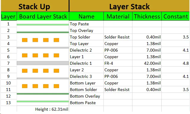
Total PCB thickness refers to the finished board measurement from one outer copper surface to the opposite outer surface. This dimension includes the core material, prepreg layers, copper foils, and any solder mask. Standard thicknesses range from 0.4 mm to 3.2 mm, with 1.6 mm being common for many hobby projects. Component compatibility depends on this value because different mounting technologies interact with the board in distinct ways. Through-hole components pass leads through drilled holes, while surface-mount devices sit on the surface pads. A mismatch between board thickness and component type can lead to mechanical stress, poor solder joints, or difficulties during automated assembly. For hobbyists building prototypes or small production runs, choosing thickness early prevents costly rework later.
Technical Principles Behind PCB Thickness and Component Mounting
Board thickness affects mechanical strength, thermal behavior, and electrical performance. Thicker boards provide greater rigidity, which benefits larger through-hole components that experience leverage forces during insertion or operation. Thinner boards flex more easily, which suits compact surface-mount layouts but may require additional support for heavier parts. Industry standards such as IPC-6012E define qualification requirements for rigid printed boards and help ensure consistent thickness tolerances across manufacturing.
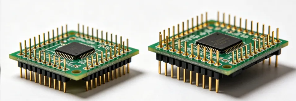
Through-hole technology relies on plated holes that extend through the entire board thickness. Leads must be long enough to protrude on the opposite side for proper soldering. Excessively thick boards demand longer leads or stepped drilling, increasing the risk of misalignment. Surface-mount devices, by contrast, attach only to one side and place fewer demands on overall thickness, though very thin boards can cause tombstoning or pad lifting during reflow. Thermal expansion differences between the board and component packages also scale with thickness. Standards such as JEDEC J-STD-020E address moisture sensitivity and reflow profiles that hobbyists should consider when selecting components for boards of varying thickness.
Practical Guidance for Selecting Components Based on PCB Thickness
Begin by defining the mechanical requirements of the project. If the design includes connectors or switches that undergo repeated insertion forces, a 1.6 mm or thicker board offers better support for through-hole mounting. For dense microcontroller boards dominated by surface-mount parts, 0.8 mm or 1.0 mm thickness often suffices and reduces overall weight. Always verify that component datasheets specify lead lengths or package heights compatible with the chosen thickness.
When mixing technologies on one board, place through-hole parts in areas where the board remains supported during soldering. Surface-mount components benefit from consistent pad design regardless of thickness, yet thinner boards may require smaller stencil apertures to control solder volume. Hobbyists using manual soldering should allow extra clearance around through-hole pads on thicker boards to accommodate larger solder fillets. Test fit components on a sample board before committing to a full order. This step reveals any clearance or lead-length issues early.
Common Issues and Troubleshooting Tips
Warpage becomes more noticeable on thinner boards during reflow, potentially lifting surface-mount pads. Maintaining even copper distribution on both sides helps minimize this effect. For through-hole parts on thick boards, ensure drill sizes accommodate lead diameters without excessive clearance that weakens the joint. If components fail to seat properly, measure actual board thickness with calipers rather than relying solely on the ordering specification.
Standards such as IPC-A-600K provide visual acceptance criteria for finished boards and help hobbyists evaluate whether thickness variations fall within acceptable limits. Checking boards upon arrival and before assembly catches most compatibility problems before soldering begins.
Conclusion
Total PCB thickness directly influences component selection and assembly success. Matching board thickness to through-hole or surface-mount requirements reduces mechanical stress and improves joint reliability. Hobbyists who consider thickness early in the design process avoid many common assembly challenges. Consistent application of industry-accepted practices leads to more robust prototypes and finished projects.
FAQs
Q1: How does PCB thickness affect through-hole component compatibility?
A1: Board thickness determines the required lead length for through-hole parts. Leads must extend fully through the board and allow proper soldering on the opposite side. Selecting components with adequate lead length for the chosen thickness prevents incomplete insertion and weak joints.
Q2: What thickness works best for SMD components on hobbyist boards?
A2: Surface-mount devices function well on boards from 0.8 mm to 1.6 mm. Thinner boards reduce weight in portable projects while still supporting standard reflow processes. Always confirm package height and thermal requirements match the board's thermal mass.
Q3: Can I mix through-hole and SMD parts on the same thickness board?
A3: Yes, mixed technology boards are common. Place through-hole components where mechanical support is strongest and ensure surface-mount pads follow standard design rules. Proper layout planning accommodates both mounting styles without thickness conflicts.
Q4: How do I verify component selection against PCB thickness?
A4: Review component datasheets for lead lengths, package dimensions, and recommended board thicknesses. Cross-check these values against the finished board specification before ordering. Sample boards allow physical testing of fit and soldering behavior.
References
IPC-6012E — Qualification and Performance Specification for Rigid Printed Boards. IPC, 2017
JEDEC J-STD-020E — Moisture/Reflow Sensitivity Classification. JEDEC, 2014
IPC-A-600K — Acceptability of Printed Boards. IPC, 2020





