ALLPCB


Introduction
High-speed digital circuits operate at frequencies where signal integrity becomes a critical concern in PCB performance. Traditional PCB materials often introduce delays and losses that degrade performance in applications like data centers, telecommunications, and computing systems. Low Dk PCB materials address these issues by offering a lower dielectric constant, which directly influences signal propagation speed and overall circuit efficiency. Engineers designing digital circuit boards must understand how these materials enhance reliability and speed. This article explores the technical impacts and practical implications of low Dk PCB in high-speed digital environments. By focusing on engineering principles, it provides structured insights for optimizing PCB performance.
What Is Low Dk PCB and Why It Matters
The dielectric constant, denoted as Dk or εr, measures a material’s ability to store electrical energy in an electric field relative to vacuum. Low Dk PCB refers to printed circuit boards fabricated with substrates having a dielectric constant typically lower than standard materials, enabling superior electrical performance. These materials minimize capacitance between traces, which is essential for maintaining signal fidelity in high-speed digital designs. In the context of high-speed PCB materials, low Dk substrates reduce phase shifts and timing skew across long traces. Industry relevance stems from the growing demand for faster data rates in digital circuit design, where even minor delays can cause errors. Selecting low Dk PCB ensures compliance with performance requirements outlined in standards like IPC-2221.
Engineers prioritize low Dk PCB because it directly correlates with reduced signal distortion in multilayer boards. As data rates exceed several gigabits per second, the choice of substrate material dictates the feasibility of routing high-speed signals without excessive loss. Low Dk materials also exhibit better stability over temperature and frequency variations, which is crucial for reliable digital circuit design. Without these properties, high-speed signals suffer from increased jitter and eye diagram closure. Thus, low Dk PCB represents a foundational element in modern high-speed applications.
Fundamental Technical Principles of Low Dk in Signal Propagation
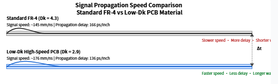
Signal propagation speed in a PCB dielectric is governed by the formula v = c / √Dk, where c is the speed of light in vacuum and Dk is the dielectric constant. A lower Dk value results in a higher propagation velocity, shortening the time signals take to travel between components. This reduction in propagation delay is vital for synchronizing clocks and data in high-speed digital circuits. For instance, halving the Dk effectively doubles the relative speed compared to higher Dk substrates, minimizing skew in differential pairs. Engineers must account for this in timing budgets during digital circuit design.
Beyond speed, low Dk materials improve characteristic impedance control, as impedance Z0 depends on √(L/C), where capacitance C scales with Dk. Stable low Dk ensures consistent Z0 across the board, reducing reflections at impedance mismatches. This principle aligns with guidelines in IPC-2141 for high-speed controlled impedance designs. Reflections cause ringing and overshoot, which degrade signal integrity at high frequencies. Therefore, low Dk PCB enhances overall PCB performance by maintaining predictable electrical behavior.
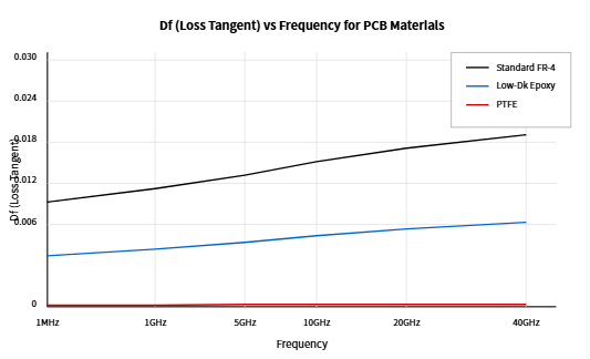
Dielectric absorption and polarization losses also decrease with low Dk, though dissipation factor Df plays a complementary role. Low Dk substrates often pair with low Df to minimize insertion loss, where signals attenuate less over distance. In high-speed digital traces, this preserves eye opening and reduces bit error rates. Measurement of Dk follows methods like IPC-TM-650 2.5.5.6, ensuring material specs meet design needs. These mechanisms collectively elevate high-speed PCB materials’ effectiveness.
Impact on Crosstalk, Loss, and Signal Integrity
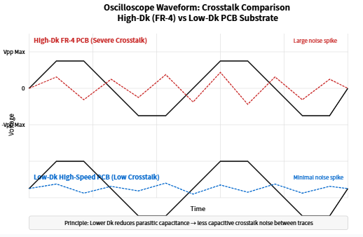
Crosstalk arises from capacitive and inductive coupling between adjacent traces, exacerbated by higher Dk values that increase fringing fields. Low Dk PCB reduces this coupling, allowing closer trace spacing without excessive near-end or far-end crosstalk. In dense digital circuit designs, this enables higher routing density while preserving signal quality. Engineers can thus optimize layer stackups for better isolation in high-speed environments.
Insertion loss, comprising conductor and dielectric components, improves significantly with low Dk materials. Dielectric loss tangent Df interacts with Dk, but lower Dk inherently lowers total loss at gigahertz frequencies. This is critical for long traces in backplanes or SerDes channels, where signals must maintain amplitude. PCB performance metrics, verified per IPC-6012, confirm these benefits through qualification tests.
Return loss and radiation are further mitigated, as low Dk supports better confinement of electromagnetic fields to the traces. In practice, simulations incorporating accurate Dk models predict these effects early in design. Overall, low Dk PCB transforms high-speed digital circuit performance by addressing multiple integrity challenges simultaneously.
Related Reading: Troubleshooting Signal Loss in High Frequency Circuits: The Role of Low Dk PCB
Design and Fabrication Best Practices for Low Dk PCB
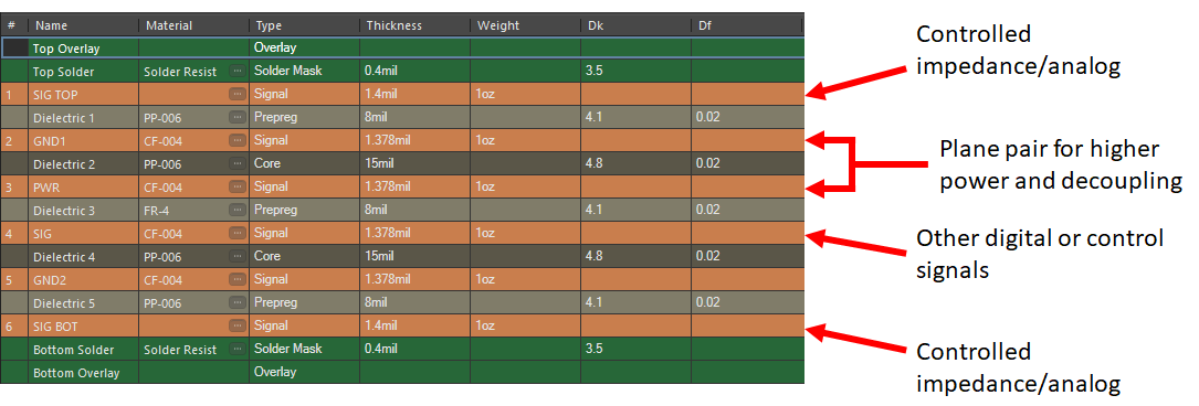
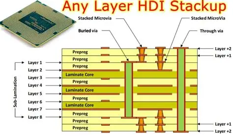
Selecting high-speed PCB materials requires balancing Dk, Df, thermal properties, and cost. Engineers should specify Dk tolerances tightly, typically within 1-2%, to ensure uniformity across panels. Stackup design must position low Dk cores strategically between signal layers for optimal propagation. Reference planes adjacent to signals further stabilize impedance, per IPC-2221 guidelines.
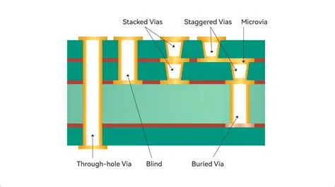
Fabrication processes demand controlled lamination to avoid resin voids that alter effective Dk. Low Dk materials often require specialized handling due to sensitivity to moisture and processing temperatures. Prepreg selection matches core Dk for homogeneous fields. Via optimization, such as backdrilling, complements material benefits by reducing stubs that cause loss.
Testing verifies performance: time-domain reflectometry for impedance, vector network analysis for loss. Compliance with IPC-6012 ensures boards meet class 3 requirements for high-reliability apps. Simulation tools model Dk variations, guiding iterations.
Routing strategies include length matching for skew control and serpentine for delay tuning, leveraging faster propagation. Ground plane partitioning isolates noisy sections. These practices maximize low Dk PCB advantages in digital circuit design.
Related Reading: Low Dk PCB Stackup Design: Optimizing Performance and Cost
Challenges and Mitigation Strategies
Low Dk materials can exhibit higher CTE mismatch with copper, risking warpage in multilayer boards. Mitigation involves symmetric stackups and constrained lamination per IPC standards. Cost is another hurdle, but performance gains justify it for high-speed needs.
Signal launch conditions at connectors benefit from low Dk, but transitions require careful modeling. Hybrid stacks blending low Dk with cost-effective layers optimize economics. Reliability testing under thermal cycling confirms stability.
Conclusion
Low Dk PCB profoundly impacts high-speed digital circuit performance by accelerating signal propagation speed, stabilizing impedance, and minimizing losses. These materials enable reliable digital circuit design at multi-gigabit rates, essential for advancing electronics. Adhering to standards like IPC-2141 and IPC-TM-650 ensures consistent results. Engineers gain structured approaches to select and implement high-speed PCB materials effectively. Ultimately, low Dk PCB elevates PCB performance, supporting next-generation applications.
FAQs
Q1: What role does low Dk PCB play in improving signal propagation speed for high-speed digital circuits?
A1: Low Dk PCB increases signal velocity via v = c / √Dk, reducing propagation delay across traces. This minimizes timing skew and supports higher data rates in digital circuit design. Stable Dk prevents frequency-dependent variations, ensuring predictable performance. Engineers verify this through simulations and tests aligned with industry methods.
Q2: How do high-speed PCB materials with low Dk affect impedance control in digital circuit design?
A2: Low Dk reduces capacitance, stabilizing characteristic impedance Z0 for reflections-free transmission. This allows precise 50-ohm or 100-ohm routing essential for high-speed signals. Per IPC-2141, controlled impedance designs benefit from uniform Dk across layers. Resulting PCB performance includes better return loss and signal fidelity.
Q3: Why is low Dk PCB critical for minimizing crosstalk in high-speed digital applications?
A3: Low Dk lowers fringing fields, decreasing capacitive coupling between traces. This permits denser routing without excessive crosstalk, vital for compact boards. Combined with ground planes, it enhances isolation in multilayer stackups. PCB performance improves, supporting error-free operation at gigabit speeds.
Q4: What best practices ensure optimal PCB performance with low Dk materials?
A4: Specify tight Dk tolerances, design symmetric stackups, and test per IPC-TM-650 2.5.5.6. Route with length matching and adjacent references for integrity. Fabrication controls prevent voids altering effective Dk. These steps optimize high-speed PCB materials in digital circuit design.
References
IPC-2221C — Generic Standard on Printed Board Design. IPC, 2023
IPC-2141A — Design Guide for High-Speed Controlled Impedance Circuit Boards. IPC
IPC-TM-650 2.5.5.6 — Full Sheet Resonance Test for Permittivity of Clad Laminates. IPC
IPC-6012F — Qualification and Performance Specification for Rigid Printed Boards. IPC, 2023