 ALLPCB


Introduction
Printed circuit boards form the backbone of modern electronic systems, and trace damage remains one of the most common failure modes encountered during manufacturing, assembly, and field operation. As component densities rise and board layers increase, traditional manual repair approaches often prove insufficient for maintaining electrical integrity and long-term reliability. Engineers now examine emerging repair technologies that combine precision energy delivery, advanced materials, and process automation to restore functionality without compromising the surrounding circuitry. These developments align with established quality frameworks that emphasize consistent workmanship and performance verification across the electronics industry.
Why PCB Trace Repair Matters in Modern Electronics
Trace repair directly influences product yield, service life, and overall system cost in high-reliability applications such as automotive controls, medical instrumentation, and aerospace electronics. When a trace opens or delaminates, the entire assembly may require replacement unless a targeted restoration method restores continuity while preserving impedance characteristics. Effective repair techniques therefore support sustainability goals by extending the usable life of complex boards rather than discarding them after minor defects appear. Industry standards such as IPC-6012E establish baseline expectations for board qualification that repair processes must meet to ensure restored sections perform equivalently to original fabrication.
Emerging Technologies for Advanced PCB Repair Methods
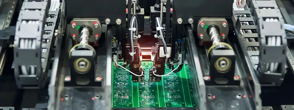
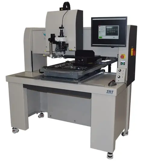
Laser-based repair systems deliver focused energy to remove oxidized material or deposit conductive filler with micrometer-level accuracy, reducing the risk of thermal damage to adjacent components. Automated repair platforms integrate machine vision and robotic positioning to identify trace faults, apply corrective material, and verify electrical continuity in a single workflow. Nano-materials, including silver nanowires and graphene-enhanced pastes, offer improved conductivity and flexibility compared with conventional solder alloys, enabling repairs on flexible substrates or high-frequency circuits where mechanical stress is a concern. These technologies collectively address the limitations of manual soldering by providing repeatable, data-driven outcomes that scale across production volumes.
Related Reading: The Ultimate Guide to PCB Trace Repair: Step by Step for Engineers
Technical Principles and Mechanisms
Laser PCB repair operates on the principle of controlled ablation and selective deposition, where pulse duration and wavelength determine the depth of material removal without affecting underlying dielectric layers. Automated PCB repair systems rely on closed-loop feedback from thermal imaging and four-point resistance measurements to adjust energy input in real time, ensuring the repaired trace meets original current-carrying capacity. Nano-materials for PCB repair function through percolation networks that form conductive paths at lower sintering temperatures, preserving the glass transition characteristics of the substrate. These mechanisms must satisfy acceptance criteria defined in IPC-A-600K to confirm that restored traces exhibit acceptable visual and electrical characteristics after repair.
Related Reading: The Art of PCB Trace Repair Using a Rework Station
Best Practices for Implementing Future Repair Techniques
Engineers begin by documenting the exact location and extent of trace damage using non-destructive inspection methods before selecting the appropriate repair technology. Process parameters such as laser fluence or nano-material curing profiles are validated against qualification samples to confirm impedance and thermal cycling performance remain within specification. Post-repair inspection includes both electrical testing and microscopic examination to verify that no new defects, such as delamination or residue, have been introduced. Documentation of each repair step supports traceability requirements and facilitates continuous improvement of repair protocols across product families.
Conclusion
The evolution of PCB trace repair continues to emphasize precision, repeatability, and material compatibility as board complexity increases. Laser PCB repair, nano-materials for PCB repair, and automated PCB repair collectively represent a shift toward data-driven restoration methods that align with the performance expectations established by IPC and related standards. Adoption of these approaches enables organizations to maintain high yields while supporting the broader goals of electronics sustainability and cost efficiency. Continued refinement of process controls and material formulations will determine how effectively the industry meets future demands for reliable, long-life electronic assemblies.
FAQs
Q1: What are advanced PCB repair methods and how do they differ from traditional techniques?
A1: Advanced PCB repair methods combine laser energy delivery, nano-scale conductive materials, and automated positioning systems to restore trace continuity with greater precision and repeatability than manual soldering. These approaches minimize thermal stress on surrounding components and allow restoration on high-density or flexible boards where conventional methods risk further damage. Engineers evaluate each method against electrical and mechanical requirements to select the most suitable process for a given failure mode.
Q2: How does laser PCB repair improve outcomes in high-reliability applications?
A2: Laser PCB repair uses controlled pulses to remove damaged material and deposit conductive filler with micrometer accuracy, preserving impedance and current-carrying capacity in critical traces. The process reduces operator variability and supports verification through integrated resistance and thermal imaging feedback. When performed according to established workmanship standards, laser repair extends board service life without introducing new failure mechanisms.
Q3: What role do nano-materials for PCB repair play in future electronics maintenance?
A3: Nano-materials for PCB repair form conductive networks at lower processing temperatures, enabling repairs on temperature-sensitive substrates and flexible circuits. Their improved mechanical flexibility helps maintain continuity under vibration or thermal cycling that would crack conventional solder joints. Validation against industry acceptance criteria ensures these materials meet the same performance thresholds as original board fabrication.
Q4: How will automated PCB repair influence the future of electronics repair?
A4: Automated PCB repair integrates vision systems and robotic control to detect, correct, and verify trace faults in a single pass, increasing throughput while reducing human error. This capability supports high-mix, low-volume production environments where manual repair becomes economically impractical. Consistent application of these systems aligns with quality management expectations and contributes to more sustainable electronics lifecycles.





