ALLPCB


High-speed printed circuit boards require careful material choices to maintain reliable signal transmission while supporting efficient manufacturing. Engineers must balance electrical performance with production constraints when selecting substrates for applications operating above several gigahertz. Proper material decisions directly influence impedance control, propagation delay, and overall system reliability. Design for manufacturability considerations ensure that chosen materials can be processed without excessive yield loss or cost escalation. This article examines the interplay between material properties, signal integrity requirements, and practical manufacturing factors.
Why Material Selection Matters for High-Speed Designs
Material selection forms a foundational step in high-speed PCB development because substrate properties govern how electromagnetic waves travel through the board. In high-frequency PCB materials, even small variations in dielectric behavior can cause measurable distortion or attenuation over trace lengths of a few inches. Procurement teams and designers evaluate these properties early to avoid costly redesigns later in the project. DFM material selection PCB practices help align electrical targets with available fabrication processes and standard panel sizes. When materials match both performance needs and manufacturing capabilities, projects achieve shorter lead times and higher first-pass yields.
Technical Principles of Signal Integrity in PCB Materials
Signal integrity depends primarily on the dielectric constant and dissipation factor of the substrate. The dielectric constant determines the speed at which signals propagate and influences the characteristic impedance of transmission lines. A higher dielectric constant slows propagation and requires narrower traces or adjusted geometries to maintain target impedance values. The dissipation factor, often called loss tangent, quantifies energy lost as heat during signal transmission. At elevated frequencies, this loss becomes more pronounced, leading to reduced amplitude and potential bit errors in digital systems.
Temperature and frequency dependence of these properties further complicate design. Many substrates exhibit changes in dielectric constant as operating conditions vary, which can shift impedance outside acceptable tolerances. Moisture absorption represents another variable that alters effective dielectric behavior and can degrade long-term reliability. Engineers therefore examine material data across the expected frequency range and environmental conditions before finalizing selections. Structured evaluation of these mechanisms supports consistent performance in high-speed applications.
DFM Considerations in Material Selection
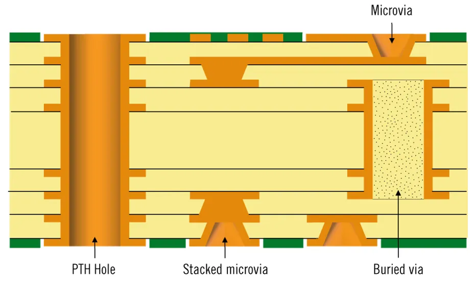
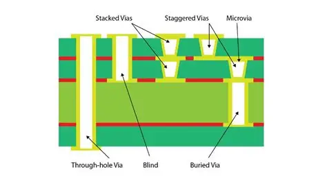
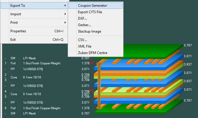
Design for manufacturability requires that chosen materials support standard etching, drilling, and lamination processes without introducing excessive defects. Materials with very low dielectric constants may demand specialized handling or thinner copper foils that increase the risk of damage during processing. Thermal expansion characteristics must align with copper and other layers to minimize warpage after reflow or thermal cycling.
Fabrication tolerances for trace width and dielectric thickness also influence achievable impedance control. Selecting materials whose properties remain stable within normal process variations reduces the need for extensive compensation in layout. When DFM material selection PCB guidelines are followed, boards can be produced on existing equipment while still meeting electrical specifications. This alignment lowers both prototype iterations and production scrap rates.
Best Practices for High-Frequency PCB Materials
Engineers begin by defining the maximum operating frequency and acceptable signal loss budget for each critical net. Materials with lower dissipation factors are prioritized when loss must remain minimal over longer trace lengths. Dielectric constant signal integrity targets are then matched to available copper weights and dielectric thicknesses that support controlled impedance routing.
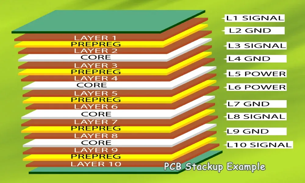
Stackup planning incorporates these material properties early so that reference planes and signal layers maintain consistent spacing. Thermal and mechanical requirements, such as glass transition temperature and coefficient of thermal expansion, receive equal attention to ensure reliability after assembly. Collaboration between design and manufacturing teams verifies that selected high-frequency PCB materials fit within standard process capabilities and panel utilization goals. Documentation of material specifications, including lot-to-lot consistency expectations, supports repeatable production outcomes.
Practical Insights from Common Design Challenges
Designers frequently encounter situations where initial material choices produce impedance values outside the required tolerance after fabrication. In such cases, reviewing the actual dielectric thickness and copper roughness against datasheet assumptions often reveals the source of deviation. Adjusting trace widths or switching to a material with tighter thickness tolerance restores compliance without major layout changes.
Another recurring issue involves excessive insertion loss at higher frequencies. Comparing measured S-parameters against predictions based on dissipation factor helps isolate whether the material or the surface finish contributes most to the loss. These structured troubleshooting steps reinforce the value of thorough material evaluation before committing to production volumes.
Conclusion
Effective material selection for high-speed PCBs integrates electrical performance targets with manufacturing realities. Attention to dielectric constant, dissipation factor, and thermal-mechanical properties supports both signal integrity and reliable production. When DFM principles guide choices from the outset, projects achieve better yields and fewer revisions. Consistent application of these considerations enables engineers to deliver robust high-frequency designs that meet both technical and commercial objectives.
FAQs
Q1: How does dielectric constant affect signal integrity in high-speed PCBs?
A1: The dielectric constant directly controls signal propagation speed and characteristic impedance. Variations in this property across frequency or temperature can cause reflections and timing skew. Selecting materials with stable dielectric constant values helps maintain consistent PCB material signal integrity throughout the operating range.
Q2: What role does DFM play in material selection for PCBs?
A2: DFM material selection PCB ensures that chosen substrates align with standard fabrication processes, including etching, drilling, and lamination. This alignment reduces warpage, improves yield, and supports achievable impedance tolerances without specialized equipment.
Q3: Which properties of high-frequency PCB materials most influence signal loss?
A3: Dissipation factor and conductor surface roughness are primary contributors to signal loss at high frequencies. Lower dissipation factor materials reduce dielectric loss, while smoother copper surfaces minimize conductor loss. Both factors must be evaluated together when specifying high-frequency PCB materials.
Q4: Why is controlled impedance important when selecting PCB materials?
A4: Controlled impedance requires precise matching of dielectric constant, trace geometry, and dielectric thickness. Material choices that support tight tolerances in these parameters enable reliable high-speed signaling and reduce the need for post-fabrication tuning.