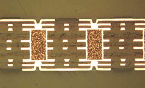
Are you an engineer looking for a reliable PCB trace repair guide for professionals? Whether you're dealing with a damaged trace on a high-density board or tackling fine-pitch repairs, this comprehensive guide has you covered. From advanced PCB trace repair techniques to the best tools for PCB trace repair, we’ll walk you through every step to restore your circuit boards effectively and efficiently.
In this detailed blog, we’ll break down the process of repairing fine-pitch PCB traces and provide actionable tips for PCB trace repair for high-density boards. Let’s dive into the world of PCB repair and equip you with the knowledge and skills to save your electronics from failure.
Why PCB Trace Repair Matters for Engineers
Printed Circuit Boards (PCBs) are the backbone of modern electronics, connecting components through intricate copper traces. When a trace gets damaged due to physical stress, corrosion, or manufacturing defects, the entire device can malfunction. For engineers, knowing how to repair these traces is a critical skill that saves time, reduces costs, and prevents the need for full board replacements.
Damaged traces can lead to signal loss, short circuits, or complete failure of the circuit. For instance, a broken trace on a high-density board carrying signals at 5 GHz could disrupt data transmission, leading to performance issues. Repairing these traces ensures continuity and maintains the integrity of impedance, often around 50 ohms for standard RF applications. This guide focuses on practical solutions tailored for professionals who need precision and reliability in their repairs.
Understanding PCB Traces and Common Damage Issues
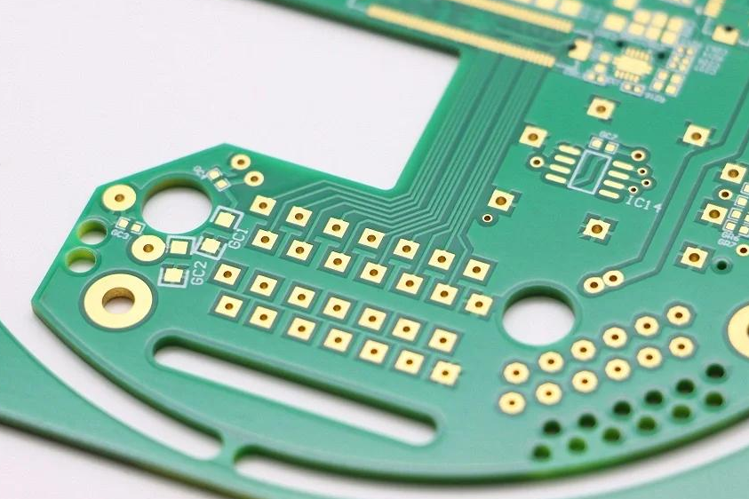
PCB traces are thin copper lines on the board that carry electrical signals between components. Their width, thickness, and spacing are critical for maintaining signal integrity and current capacity. For example, a trace width of 0.2 mm might carry up to 1 amp of current, depending on the copper thickness (typically 1 oz or 35 μm).
Common issues with PCB traces include:
- Physical Breaks: Caused by mechanical stress or impact, leading to open circuits.
- Corrosion: Exposure to moisture or chemicals can degrade copper traces over time.
- Burnt Traces: Overcurrent or short circuits can cause traces to overheat and burn, disrupting connectivity.
- Delamination: On multilayer boards, traces can separate from the substrate due to poor manufacturing or thermal stress.
Understanding the type of damage is the first step in choosing the right repair method, especially for complex boards with fine-pitch traces or high-density layouts.
Essential Tools for PCB Trace Repair
Before starting any repair, having the right tools is crucial for precision and safety. Here are the best tools for PCB trace repair that every engineer should have in their toolkit:
- Soldering Iron with Fine Tip: A temperature-controlled iron with a 1 mm or smaller tip for precise soldering on fine-pitch traces.
- Desoldering Wick and Pump: For removing old solder without damaging nearby components.
- Multimeter: To test continuity and identify breaks in traces with accuracy down to 0.1 ohms.
- Magnifying Glass or Microscope: Essential for inspecting fine-pitch traces, especially on high-density boards with spacing as tight as 0.1 mm.
- Conductive Epoxy or Repair Pens: For quick fixes on small trace breaks, offering conductivity and ease of application.
- X-Acto Knife or Scalpel: To carefully scrape away solder mask or debris without damaging adjacent traces.
- Isopropyl Alcohol and Brush: For cleaning the repair area to ensure proper adhesion and prevent contamination.
- Fiberglass Scratch Brush: To remove oxidation from copper traces before repair.
Investing in high-quality tools ensures that repairs are done cleanly and effectively, minimizing the risk of further damage to the board.
Related Reading: How to Repair a Damaged PCB Trace: A Step-by-Step Guide
Step-by-Step PCB Trace Repair Guide for Professionals
Now that you have the necessary tools, let’s walk through a detailed process for repairing damaged PCB traces. This PCB trace repair guide for professionals is designed to be practical and easy to follow, even for complex repairs.
Step 1: Assess the Damage
Use a magnifying glass or microscope to closely inspect the damaged trace. Identify whether it’s a complete break, a partial crack, or a burnt section. Use a multimeter to confirm the break by testing for continuity. For high-density boards, ensure you’re examining the correct layer if it’s a multilayer design.
Step 2: Clean the Area
Remove any debris, solder mask, or oxidation around the damaged trace using a scalpel and a fiberglass brush. Clean the area with isopropyl alcohol and a small brush to ensure a contaminant-free surface. This step is critical for ensuring a strong bond during the repair.
Step 3: Expose the Copper (If Necessary)
If the trace is covered by solder mask, carefully scrape it away with a scalpel to expose the copper underneath. Be gentle to avoid cutting into adjacent traces, especially on boards with fine-pitch spacing as small as 0.15 mm.
Step 4: Choose the Repair Method
Depending on the damage, select the appropriate repair technique:
- For Small Breaks: Apply conductive epoxy or use a conductive repair pen to bridge the gap. These materials have resistances as low as 0.01 ohms per square, suitable for low-current signals.
- For Larger Breaks: Solder a thin wire (e.g., 30 AWG) across the break to restore connectivity. Use flux to ensure a clean solder joint.
- For Burnt Traces: Remove the damaged section and replace it with a jumper wire, securing it with solder at both ends.
Step 5: Secure the Repair
After bridging the gap, apply a small amount of epoxy or UV-curable solder mask over the repaired area to protect it from environmental factors. This step is especially important for boards exposed to humidity or vibration.
Step 6: Test the Repair
Use a multimeter to check for continuity across the repaired trace. Additionally, power up the board (if safe) to ensure the circuit functions as expected. For high-frequency signals, verify that the repair hasn’t introduced unwanted impedance mismatches beyond the typical 50-ohm standard.
Related Reading: PCB Trace Repair for Beginners: A Hobbyist's Guide to Saving Damaged Boards
Advanced PCB Trace Repair Techniques for Complex Boards
For engineers working on sophisticated designs, advanced PCB trace repair techniques are often necessary. These methods address challenges like multilayer boards, fine-pitch components, and high-frequency signals.
Repairing Fine-Pitch PCB Traces
Repairing fine-pitch PCB traces requires precision due to the tight spacing between traces, sometimes as small as 0.1 mm. Use a microscope for visibility and a soldering iron with a 0.5 mm tip. Avoid excess solder to prevent bridging between adjacent traces. If a trace is damaged near a component pad, consider desoldering the component first to access the area safely.
PCB Trace Repair for High-Density Boards
PCB trace repair for high-density boards often involves multilayer designs where traces are hidden between layers. Use a schematic or X-ray inspection to locate internal breaks if possible. For surface repairs, follow the standard steps but prioritize minimal heat application to avoid delaminating layers. A hot air rework station with a temperature setting of 300°C can help if soldering near sensitive components.
Handling High-Frequency Signal Traces
For traces carrying high-frequency signals (e.g., above 1 GHz), repairs must maintain signal integrity. Avoid long jumper wires that could act as antennas and introduce noise. Instead, use short, direct connections and match the trace width to maintain impedance, typically 50 ohms for RF applications. Post-repair, test with an oscilloscope to ensure signal quality.
Tips for Preventing Future PCB Trace Damage
While repairs are valuable, preventing trace damage in the first place is even better. Here are some practical tips for engineers:
- Design with Redundancy: Include wider traces or redundant paths for critical signals during the design phase to handle higher currents (e.g., 2 amps for a 0.5 mm trace).
- Use Protective Coatings: Apply conformal coating to shield traces from moisture and corrosion, extending the board’s lifespan.
- Avoid Mechanical Stress: Secure PCBs properly in enclosures to prevent flexing or impact damage during operation.
- Monitor Current Loads: Ensure traces are not overloaded by adhering to current capacity guidelines during design and testing.
Common Challenges in PCB Trace Repair and How to Overcome Them
Even with the best preparation, challenges can arise during PCB trace repair. Here are some common issues and solutions:
- Adjacent Trace Damage: Use kapton tape to mask nearby traces before soldering to prevent accidental shorts.
- Heat Damage to Components: Apply heat sinks or use a low-temperature soldering iron (around 250°C) when working near sensitive parts.
- Poor Adhesion of Repair Material: Ensure the surface is thoroughly cleaned and free of oxidation before applying conductive epoxy or solder.
Conclusion: Mastering PCB Trace Repair for Professional Results
Repairing PCB traces is a vital skill for engineers, whether you’re working on simple single-layer boards or complex high-density designs. By following this PCB trace repair guide for professionals, you can confidently tackle any trace damage using advanced PCB trace repair techniques. With the best tools for PCB trace repair and a methodical approach, challenges like repairing fine-pitch PCB traces or handling PCB trace repair for high-density boards become manageable tasks.
Equipped with these step-by-step instructions and practical tips, you’re ready to restore functionality to damaged boards and extend the life of your electronics. Keep practicing these techniques to refine your skills, and always prioritize precision and safety in every repair job.
 ALLPCB


