 ALLPCB


Introduction
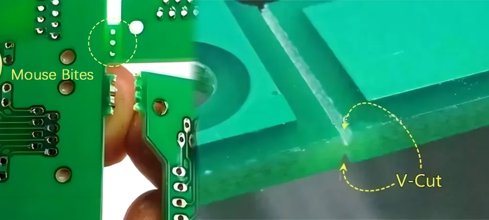
Printed circuit board panelization remains a foundational process in electronics manufacturing because it enables multiple individual boards to be processed together on a single larger panel. This approach improves handling efficiency during fabrication, assembly, and testing while reducing material waste and labor costs. Mouse bite technology, which relies on arrays of small perforations or slots along the board edges, provides a controlled method for separating those individual boards after processing. Recent developments focus on refining perforation patterns, integrating automation, and aligning designs more closely with evolving production requirements. These changes support higher throughput and better consistency across batches.
What Is PCB Panelization and Why Mouse Bite Designs Matter
PCB panelization arranges multiple circuit boards onto one standard-size panel so that all boards undergo the same sequence of drilling, plating, etching, and soldering operations. Mouse bite designs create deliberate weak points through patterns of small holes or elongated slots that allow clean separation without excessive force or damage to traces and components. The technique supports high-volume production runs where manual or automated depanelization must occur quickly and repeatably. Industry trends show increasing demand for panel layouts that accommodate denser component placement and thinner substrates while maintaining structural integrity during handling. Effective mouse bite configurations therefore contribute directly to yield improvements and reduced scrap rates in modern facilities.
Technical Principles of Advanced Mouse Bite Designs
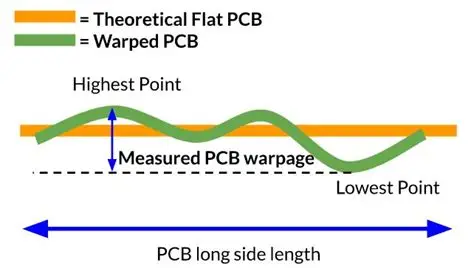
Mouse bite perforations function by locally reducing the cross-sectional area of the connecting material between boards, creating predictable fracture lines under applied stress. Engineers calculate hole diameter, spacing, and row count to balance ease of separation against the risk of premature cracking or edge burrs. Material properties such as copper thickness, laminate resin content, and glass weave orientation influence how stress propagates through the perforations. New panelization techniques often incorporate staggered or offset hole patterns to distribute mechanical loads more evenly and minimize warpage during thermal cycles. These designs also consider the interaction with automated depanelization equipment that applies consistent force or uses routing tools along the weakened lines.
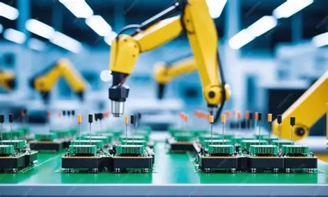
Innovations Driving Smart PCB Manufacturing
Automation has become central to depanelization because manual breaking introduces variability and potential damage. Advanced mouse bite designs now integrate features such as alignment fiducials and reinforced tab sections that guide robotic systems or laser cutters with greater precision. Industry trends emphasize data-driven optimization where panel layouts are simulated for stress distribution before fabrication begins. Some approaches combine traditional perforations with partial-depth routing or scoring to achieve cleaner edges on high-density boards. These refinements support the shift toward smart PCB manufacturing environments that track each panel through the production line and adjust parameters in real time based on measured board characteristics.
Best Practices for Implementing New Panelization Techniques
Design teams begin by reviewing board dimensions, component placement density, and expected handling forces to select appropriate mouse bite parameters. Maintaining adequate clearance between perforations and copper features prevents trace damage during separation. Testing under simulated production conditions verifies that separation forces remain within acceptable limits and that edge quality meets visual and dimensional criteria. Collaboration between design and manufacturing groups ensures that panelization layouts accommodate both current equipment capabilities and anticipated future automation upgrades. Documentation of chosen patterns and any deviations from standard practices supports consistent results across multiple production lots.
Quality Considerations and Industry Standards Alignment
Quality control procedures evaluate panel flatness, perforation uniformity, and post-separation edge condition to confirm compliance with established acceptance criteria. Standards such as IPC-6012E provide guidance on qualification and performance requirements for rigid printed boards, including aspects relevant to panel integrity. Separate evaluation against IPC-A-600K addresses visual and dimensional acceptability of the finished boards after depanelization. These references help teams establish consistent acceptance limits without introducing unnecessary conservatism that could complicate separation.
Conclusion
Mouse bite technology continues to evolve as manufacturers seek higher efficiency and reliability in panelization processes. Refinements in perforation geometry, combined with automated depanelization methods, address the demands of denser layouts and thinner materials. Structured design reviews and adherence to recognized standards support repeatable outcomes while accommodating new equipment capabilities. Ongoing attention to these elements positions facilities to meet both current production goals and emerging industry requirements.
FAQs
Q1: What advantages do new panelization techniques offer compared with traditional methods?
A1: New panelization techniques improve material utilization and enable higher board densities on standard panels. They also facilitate smoother integration with automated depanelization systems that reduce manual handling. Engineers can optimize perforation patterns to lower separation forces while preserving board integrity. These changes contribute to higher overall yields in high-volume manufacturing environments.
Q2: How do advanced mouse bite designs support automated depanelization?
A2: Advanced mouse bite designs incorporate precise hole spacing and alignment features that match the tolerances of robotic or laser-based separation equipment. The patterns reduce the risk of uneven breaks or component stress during high-speed operations. Consistent perforation geometry allows equipment parameters to remain stable across different board types. This alignment improves throughput and repeatability in smart PCB manufacturing lines.
Q3: Why are industry trends favoring refined mouse bite technology?
A3: Industry trends reflect the need for faster production cycles and reduced scrap in electronics assembly. Refined mouse bite technology allows thinner and more complex boards to be processed without compromising edge quality. Automation compatibility further reduces labor content and variability. Facilities adopting these approaches can respond more flexibly to changing product mixes and volume requirements.
Q4: What factors should engineers consider when selecting mouse bite parameters?
A4: Engineers evaluate substrate thickness, copper weight, and component proximity to the panel edges. They also assess expected mechanical stresses during handling and separation. Simulation tools help predict stress distribution and identify potential weak points before fabrication. Final selections are validated through prototype runs that confirm both separation ease and post-depanelization quality.
References
IPC-6012E - Qualification and Performance Specification for Rigid Printed Boards. IPC, 2017
IPC-A-600K - Acceptability of Printed Boards. IPC, 2020


