ALLPCB


Introduction
Stencil thickness plays a central role in achieving reliable solder joints during surface mount technology assembly. For electronic hobbyists working on their own printed circuit boards, understanding this parameter helps prevent common issues such as insufficient solder volume or bridging between pads. Proper stencil selection supports consistent paste deposition across a range of component sizes and board layouts. This knowledge directly improves first pass yield and reduces rework time on prototype builds. Many hobbyists discover that adjusting stencil thickness early in the design process leads to smoother assembly outcomes overall.
What Is PCB Stencil Basics and Why It Matters
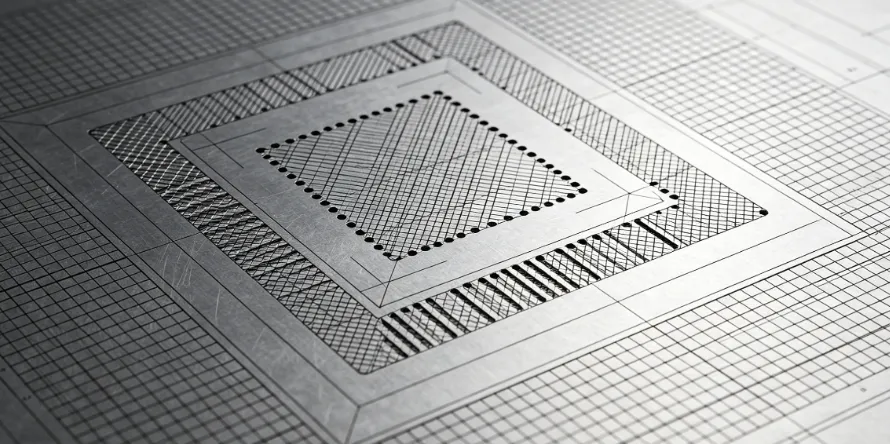
A PCB stencil is a thin metal sheet with precisely cut apertures that allow solder paste to be applied only to the designated pads on a board. Stencil thickness determines the volume of paste deposited during the printing step of SMT assembly. For beginners, this choice influences how well components adhere after reflow and whether the final joints meet mechanical and electrical requirements. In hobbyist projects involving mixed component pitches, the wrong thickness often results in open circuits or excess paste that causes shorts. Following established industry practices helps hobbyists avoid these pitfalls and produce boards that function reliably from the first assembly run.
Technical Principles Behind Stencil Thickness
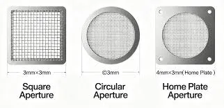
The amount of solder paste transferred through each aperture depends on the relationship between stencil thickness and aperture geometry. Thicker stencils deliver more paste volume, which benefits larger components that require stronger mechanical bonds. Thinner stencils reduce volume and improve release characteristics on fine pitch features where excess paste could bridge adjacent pads. Surface tension and paste rheology interact with the stencil walls during squeegee travel, affecting transfer efficiency. According to IPC-7525 guidelines, designers evaluate area ratio and aspect ratio to predict how well paste will release from the apertures. These principles guide hobbyists in matching stencil properties to the specific demands of their component mix and board layout.
Related Reading: Decoding Stencil Thickness: A Comprehensive Guide for PCB Assembly Success
Practical Solutions and Best Practices for SMT Assembly Tutorial
Hobbyists begin by reviewing the component data sheets and pad layouts to identify the finest pitch features on the board. A single stencil thickness is then chosen that balances paste volume across all pads while maintaining acceptable release on the smallest apertures. Step stencils with localized thickness variations offer one practical workaround when a design includes both large power components and fine pitch integrated circuits. During solder paste application, consistent squeegee pressure and speed help ensure uniform deposition regardless of the chosen thickness. Testing a small number of boards with the selected stencil reveals any needed adjustments before committing to a full production run. These steps form the core of an effective SMT assembly tutorial for anyone building boards at home or in a small workshop.
Related Reading: Step Stencil Thickness: How to Determine the Ideal Value for Your PCB

Troubleshooting Common Issues in Solder Paste Application
When paste volume appears too low after printing, the first check is whether the stencil thickness matches the requirements of the smallest components. Insufficient paste often leads to weak joints that fail during thermal cycling or mechanical stress. Conversely, excessive thickness on fine pitch areas produces bridging that requires manual cleanup. Hobbyists troubleshoot by inspecting the first few prints under magnification and measuring paste height where possible. Adjusting aperture sizes in the stencil design or switching to a different thickness usually resolves the imbalance without major board changes. Consistent documentation of each trial helps refine the process for future projects.
PCB Design for Manufacture Considerations
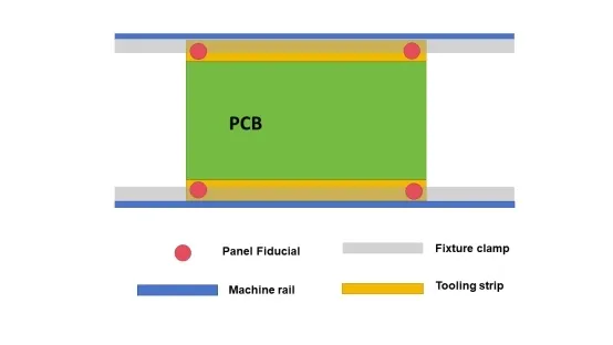
Early collaboration between schematic capture and stencil planning prevents costly revisions later. Designers incorporate fiducial marks and adequate clearance around pads to support accurate stencil alignment during printing. When boards contain both through hole and surface mount parts, the stencil must accommodate the surface mount areas without interfering with other features. Following these PCB design for manufacture practices reduces the chance of assembly defects that only appear after reflow. Hobbyists who plan stencil thickness alongside pad sizing and component placement achieve more predictable results on every build.
Conclusion
Selecting the right stencil thickness forms a foundational skill for anyone performing SMT assembly at the hobby level. By understanding how thickness affects paste volume and release, hobbyists can avoid many common defects and improve overall board quality. Practical testing combined with attention to component requirements leads to consistent, reliable outcomes. Applying these principles during the design phase further streamlines the entire manufacturing workflow.
FAQs
Q1: What factors determine the best stencil thickness for beginners working with PCB stencil basics?
A1: Stencil thickness selection starts with the range of component pitches on the board and the desired solder volume for each pad. Hobbyists review their layout to find the smallest features and choose a thickness that supports good paste release while still providing enough material for larger parts. Practical testing on sample boards confirms the choice before full assembly.
Q2: How does stencil thickness affect solder paste application in an SMT assembly tutorial?
A2: Thicker stencils deposit more paste, which helps larger components form strong joints, while thinner stencils improve accuracy on fine pitch pads. During printing, the chosen thickness influences how cleanly the paste releases from the apertures. Hobbyists adjust pressure and speed to match the stencil and achieve uniform deposits across the board.
Q3: Why is stencil thickness important in PCB design for manufacture?
A3: Stencil thickness directly influences assembly yield and the need for rework. Early consideration during layout helps ensure that pad sizes and clearances support the selected stencil. This approach reduces defects such as insufficient solder or bridging and supports smoother production for hobbyist projects.
Q4: What troubleshooting steps help when solder paste application fails due to stencil thickness?
A4: Inspect printed boards under magnification to identify whether paste volume is too low or too high on specific pads. Compare results against the component pitch requirements and consider a different thickness or aperture modification. Repeating a small test run after adjustments usually identifies the correct setting for reliable joints.
References
IPC-7525C — Stencil Design Guidelines. IPC
J-STD-005 — Requirements for Soldering Pastes. IPC