 ALLPCB


What Is Solder Joint Rework and Why It Matters
Solder joint rework involves the targeted removal and replacement of solder to restore proper electrical and mechanical connections on a printed circuit board. This process becomes necessary when defects arise during initial assembly or after field use. Common issues include cold solder joint formations, solder bridges, and insufficient solder deposits that disrupt circuit continuity. Addressing these defects promptly supports consistent performance in electronic devices across various applications. Engineers rely on systematic inspection and repair techniques to prevent failures that could affect downstream manufacturing steps.
Causes of Common Solder Joint Defects
Several factors contribute to the formation of defective solder joints during surface mount technology processes. Temperature inconsistencies during reflow can lead to cold solder joint conditions where the solder fails to achieve full wetting on component leads or pads. Excessive solder paste application often creates solder bridge defects that short adjacent conductors. Insufficient solder volume results from stencil misalignment or paste deposition errors, leaving weak connections vulnerable to mechanical stress. Component placement inaccuracies and board warpage further exacerbate these problems by altering the intended solder fillet geometry. Understanding these root causes enables targeted adjustments in the assembly line to minimize recurrence.
Identifying Defects Through Inspection Methods
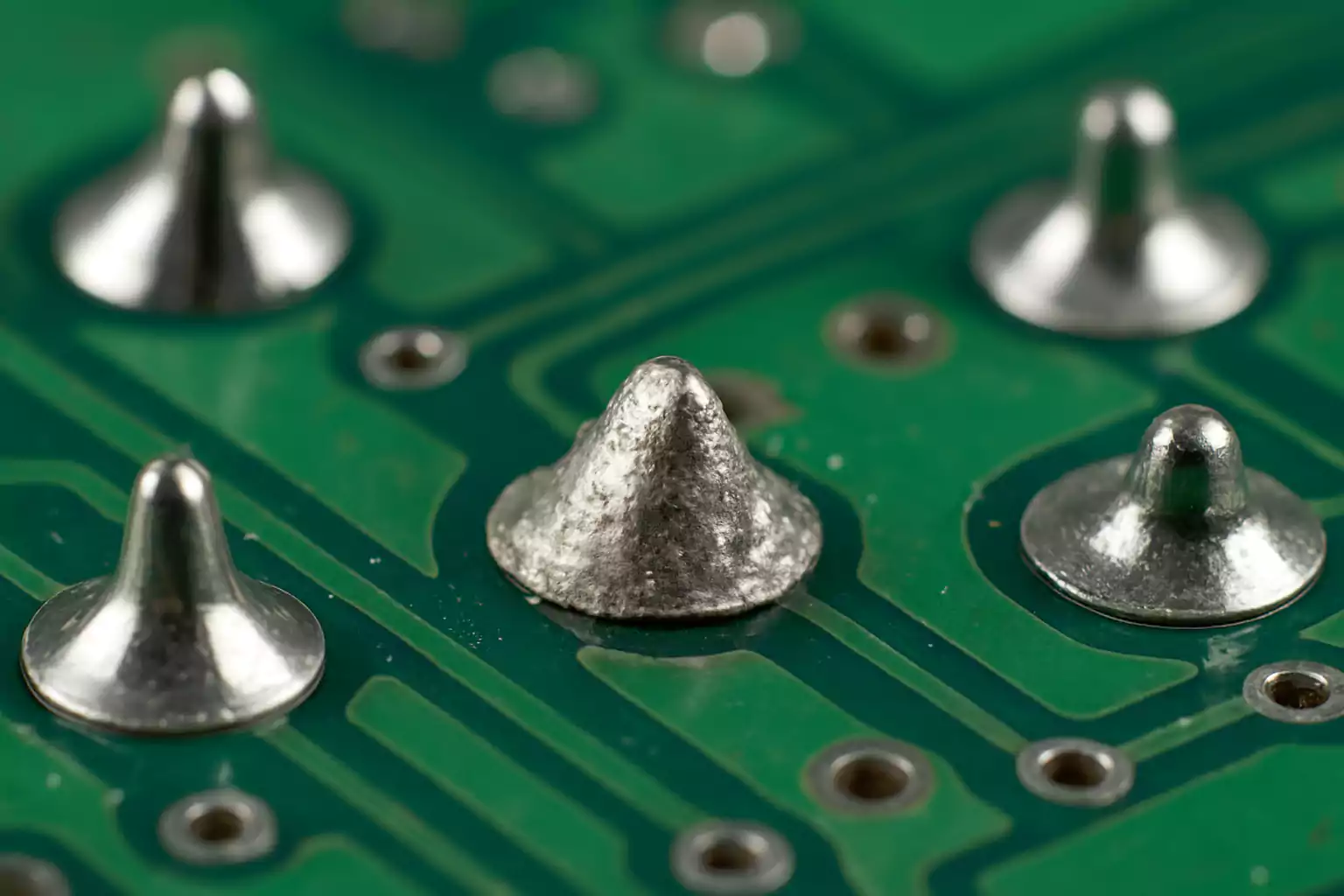
Visual inspection under magnification remains the first practical step in detecting solder joint issues. Technicians look for visual cues such as dull or cracked surfaces that indicate a cold solder joint or irregular shapes that signal a solder bridge. X-ray imaging provides additional clarity for hidden defects like insufficient solder beneath ball grid array packages. Automated optical inspection systems help flag anomalies consistently across high-volume production runs. These methods allow engineers to prioritize boards for rework based on defect severity and location.
Related Reading: Rework Rescue: Expert Techniques for Removing Pesky Solder Bridges
Correcting Defects with Targeted Rework Techniques
Once defects are identified, reflowing solder offers a direct method to correct many issues without full component removal. A controlled heat source melts the existing solder while flux improves flow and removes oxides. For more severe cases such as solder bridges, desoldering tools or braid remove excess material before fresh solder is applied. Insufficient solder joints benefit from precise addition of new solder paste followed by localized reflow to build proper fillet height. Throughout these steps, maintaining steady hand or tool control prevents further damage to surrounding components or the board substrate. Documentation of each repair ensures traceability for quality records.
Best Practices for Effective Solder Joint Repair
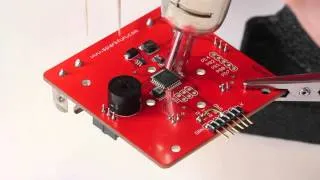
Successful solder joint repair depends on following established process controls that align with industry standards such as IPC J-STD-001. Preheating the board reduces thermal shock and improves solder flow during rework operations. Selecting the correct flux type and solder alloy matches the original assembly materials and prevents compatibility issues. Post-repair cleaning removes residues that could cause corrosion or electrical leakage over time. Regular calibration of rework equipment maintains consistent temperatures and airflow settings across multiple operators. These practices collectively improve first-pass yield and reduce the need for repeated interventions.
Related Reading: Troubleshooting Cold Solder Joints? Hot Air Rework to the Rescue!
Conclusion
Solder joint rework addresses critical defects that arise in printed circuit board assembly through systematic identification and correction methods. Engineers who apply practical troubleshooting steps achieve reliable connections while preserving board integrity. Consistent application of inspection techniques and controlled repair processes supports higher overall product quality. Ongoing attention to process variables further reduces defect rates in future production cycles.
FAQs
Q1: What causes a cold solder joint during assembly?
A1: A cold solder joint typically forms when insufficient heat prevents proper melting and wetting of the solder alloy on component leads and pads. Factors such as uneven reflow profiles, poor flux activity, or contaminated surfaces contribute to this defect. Engineers often detect it through visual inspection showing a dull, cracked appearance rather than a smooth shiny fillet. Addressing root causes in the reflow process helps prevent recurrence in subsequent builds.
Q2: How do you perform solder joint rework for a solder bridge?
A2: Solder joint rework for a bridge begins with careful removal of excess solder using desoldering braid or a vacuum tool while applying flux to aid flow. Technicians then inspect the area to confirm separation of adjacent conductors before applying fresh solder if needed. Controlled heating during reflowing solder ensures clean joints without disturbing nearby components. This targeted approach restores electrical isolation while maintaining mechanical strength.
Q3: When is reflowing solder recommended for insufficient solder defects?
A3: Reflowing solder works well for insufficient solder when the existing joint shows incomplete coverage but remains accessible for localized heating. Adding a small amount of solder paste and flux before applying controlled heat builds the required fillet volume. Engineers verify the repair through magnification to confirm proper wetting and height. This method minimizes component disturbance compared to full removal and replacement.
Q4: What inspection steps follow solder joint repair?
A4: After solder joint repair, technicians perform visual checks under magnification to confirm smooth fillets and absence of bridges or cracks. Electrical testing verifies continuity and resistance values meet design requirements. Additional X-ray review may be used for complex packages to ensure hidden joints are sound. These steps provide confidence that the reworked assembly will perform reliably in operation.





