 ALLPCB


Introduction
Electronics hobbyists often seek ways to pack more functionality into smaller spaces without sacrificing performance. Via-in-pad PCBs offer a practical solution for achieving compact designs that rival professional products. This technique places vias directly beneath component pads, enabling denser routing and multilayer connections in tiny footprints. For DIY electronics projects, via-in-pad project ideas open up possibilities like wearable sensors or LED arrays that fit in your palm. These boards support fine-pitch components and improve signal integrity, making them ideal for simple PCB projects. Exploring via-in-pad applications can elevate your next electronics hobby projects from basic prototypes to polished creations.
What Is Via-in-Pad and Why It Matters for Hobbyists
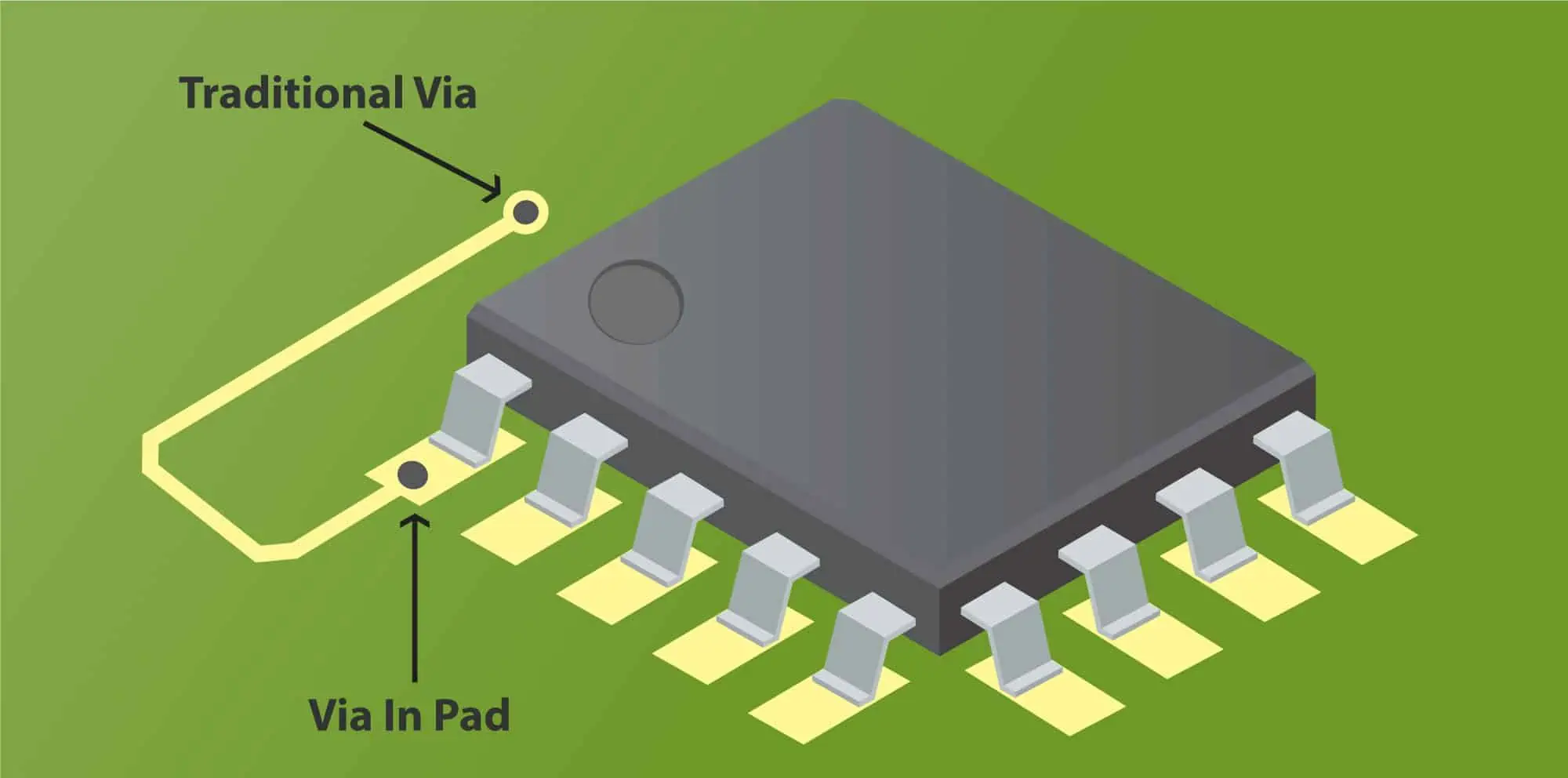
Via-in-pad refers to a PCB manufacturing process where a via hole is drilled directly into the landing pad of a surface-mount component. The via is then filled with conductive or non-conductive material and plated over to create a flat, solderable surface. This differs from traditional vias placed adjacent to pads, which consume extra board real estate. In electronics hobby projects, this method maximizes space for routing traces between layers, allowing hobbyists to design multilayer boards under 50 square millimeters. It also aids thermal dissipation by channeling heat from power components to inner planes.
The relevance grows with the rise of small SMD parts like 0402 resistors or QFN packages in DIY electronics projects. Hobbyists benefit from reduced board size, which simplifies enclosures and battery integration. Via-in-pad supports higher component density without dogbone routing, cutting design time. For simple PCB projects, it ensures reliable interlayer connections under mechanical stress. Standards like IPC-4761 outline via protection requirements, ensuring these features meet reliability thresholds even in home assemblies.
Technical Principles of Via-in-Pad PCBs
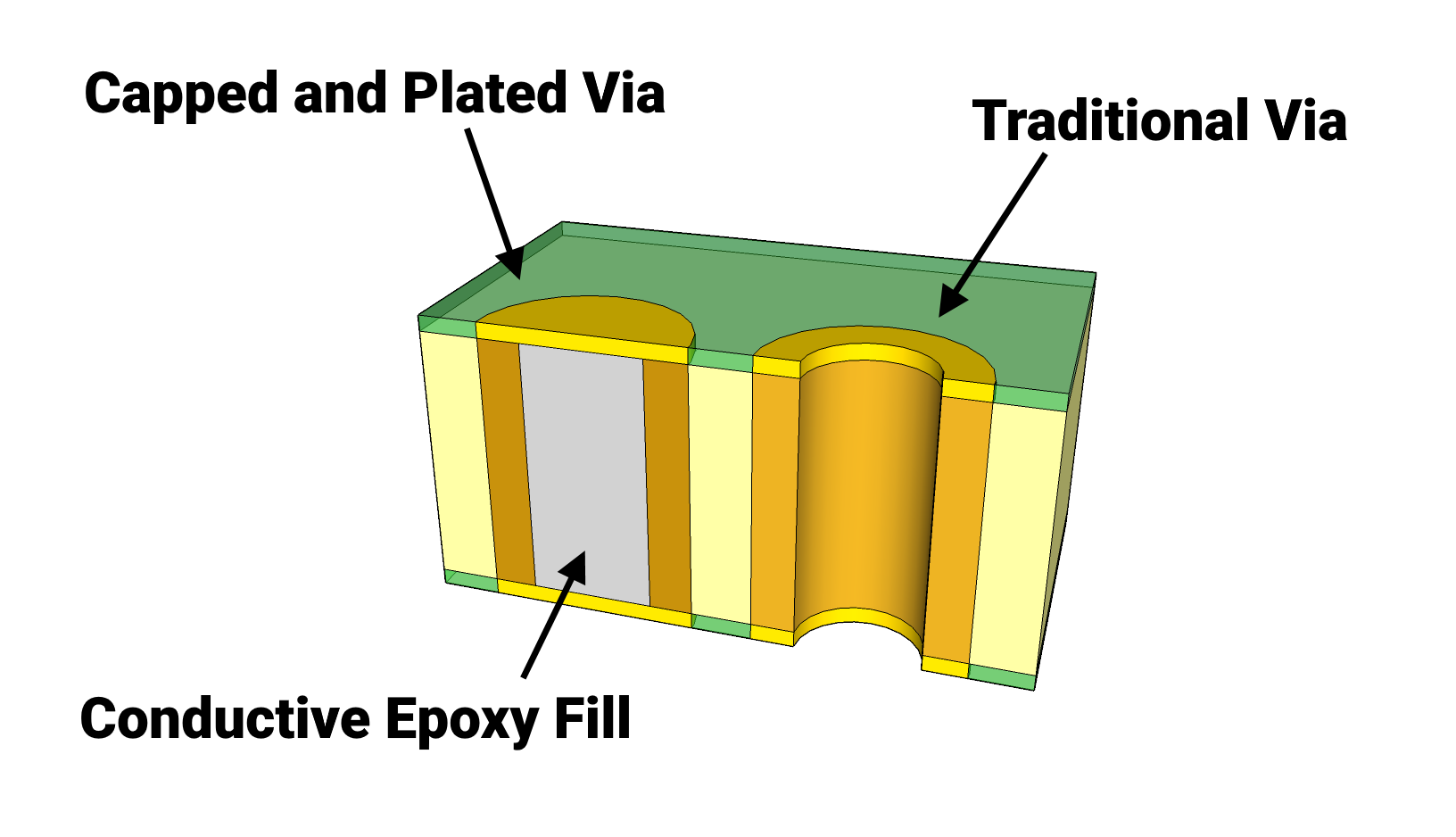
The core mechanism starts with precise drilling of the via hole within the pad boundary, followed by plating to form a conductive barrel. Filling prevents solder wicking during reflow and maintains coplanarity for component attachment. Copper filling provides superior thermal and electrical conductivity, while epoxy fill suffices for signal vias. Plating over the filled via creates a seamless pad extension, compatible with automated assembly. This process demands controlled aspect ratios to avoid plating voids, typically under 1:1 for hobby-scale boards.
Reliability hinges on fill quality and plating thickness, governed by IPC-6012 for rigid board performance. Thermal expansion mismatches between fill and copper can cause cracks if not managed, so designers select matched CTE materials. In multilayer stacks, via-in-pad enables stacked vias for HDI-like density without microvia costs. Electrical performance improves with shorter current paths, reducing inductance in high-frequency circuits. For hobbyists, understanding these principles prevents common failures like delamination during soldering.
Signal integrity benefits from minimized stub lengths, crucial for hobby RF projects like Bluetooth modules. Mechanical stability comes from the plugged structure resisting vibration in portable devices. Manufacturing involves tenting the via before filling, ensuring no resin bleed during lamination. Testing verifies fill density via X-ray or cross-sectioning, aligning with J-STD-001 assembly guidelines. These principles make via-in-pad a go-to for via-in-pad applications in constrained layouts.
Practical Via-in-Pad Project Ideas for Electronics Hobbyists
Start with a dense LED matrix driver, perfect for simple PCB projects. Use via-in-pad under shift register pads to route control signals to a ground plane, enabling a 16x16 array on a credit-card-sized board. This setup dissipates heat from current-limiting resistors efficiently. Hobbyists can program it for scrolling displays or animations using a microcontroller. The compact footprint fits custom cases, inspiring via-in-pad project ideas for signage or wearables.
Next, build a USB-powered sensor hub for environmental monitoring in DIY electronics projects. Place vias in pads of the microcontroller and sensor footprints to connect power and data layers tightly. This reduces noise pickup in analog readings from temperature or humidity sensors. A single USB Type-C connector powers multiple channels, with via-in-pad aiding plane stitching for EMI shielding. Troubleshooting tip: Ensure copper fill for power vias to handle 500mA bursts without hotspots.
A miniature audio amplifier board showcases via-in-pad for thermal management. Vias under the Class-D amp IC pad transfer heat to a bottom heatsink plane, preventing thermal shutdown in portable speakers. Route audio inputs via inner layers, using pad vias for clean signal paths. This electronics hobby project amplifies line-level sources to drive small drivers, ideal for headphones. Best practice: Space vias evenly under hot components per thermal via arrays.
For power enthusiasts, a battery charger module uses via-in-pad to stack charging ICs and protection circuits densely. Connect balance leads through pad vias to a sense plane, minimizing trace lengths for accuracy. This simple PCB project supports LiPo cells with LED status indicators. It fits drone or RC applications, where size constraints demand via-in-pad applications. Watch for solder paste volume to avoid bridging fine-pitch pads.
An RGB LED controller strip driver leverages via-in-pad for daisy-chaining multiple channels. Place vias in MOSFET pads for fast switching to inner power planes, supporting high-current LEDs. Program via SPI for effects like rainbows or music sync. This DIY electronics project powers addressable strips in home decor. Common issue: Overheating; use filled vias and add thermal reliefs.
Best Practices and Troubleshooting for Hobby Via-in-Pad Designs
Specify via fill type in your Gerber files, opting for copper in power paths and epoxy for signals. Maintain annular ring per IPC-2221 design guidelines to ensure plating integrity. Use design rule checks for via-to-pad overlap exceeding 0.1mm. For assembly, apply sufficient solder paste but avoid excess to prevent wicking in unfilled vias. Reflow profiles should match component tolerances, slowing ramps for fill stability.
Troubleshoot open vias with continuity tests post-plating. If delamination occurs, verify CTE compatibility between layers. For hobbyists, prototype on 2-layer boards first before multilayer. Panelize designs for cost efficiency in small runs. These steps ensure reliable via-in-pad project ideas without pro tools.
Conclusion
Via-in-pad PCBs transform simple PCB projects into compact powerhouses for electronics hobbyists. From LED matrices to sensor hubs, these designs deliver professional density and performance. Key benefits include space savings, thermal control, and routing flexibility. Adhering to standards like IPC-4761, IPC-6012, and J-STD-001 guarantees success. Experiment with these via-in-pad applications to spark your creativity. Your next DIY electronics project awaits a smaller, smarter board.
FAQs
Q1: What are via-in-pad project ideas suitable for beginners in electronics hobby projects?
A1: Via-in-pad works well for compact LED drivers or sensor boards where space is tight. Start with a 2-layer design placing vias under SMD pads for layer transitions, and use filled vias to avoid solder wicking during hand assembly. This enables simple PCB projects like USB gadgets without sprawling traces. Follow basic annular ring and clearance rules for reliability.
Q2: How does via-in-pad improve DIY electronics projects?
A2: It allows denser component placement, shrinking board size for wearables or tight enclosures. Vias connect layers directly under pads, freeing surface area for parts. Thermal benefits help cool power ICs via inner planes, and shorter current paths can improve signal integrity. Specify appropriate via filling per IPC guidelines to ensure solderability and reliability.
Q3: Are via-in-pad applications practical for simple PCB projects at home?
A3: Yes, especially for compact builds like audio amplifiers or USB sensor boards. Use copper-filled vias for heat paths under ICs and tent soldermask over vias to aid hand soldering. Via-in-pad can reduce layer count versus dogbone fanouts. Validate connections with a multimeter and inspect for solder bridging on fine-pitch pads.
Q4: What standards guide via-in-pad in hobby designs?
A4: IPC-4761 covers via covering and protection methods, IPC-6012 defines qualification and performance for rigid boards, and J-STD-001 provides assembly requirements. Applying these helps ensure plating, fill quality, and soldering reliability suitable for hobby-scale runs.
References
IPC-4761 - Via Protection and Covering Requirements for Printed Boards. IPC, 2020
IPC-6012E - Qualification and Performance Specification for Rigid Printed Boards. IPC, 2017
J-STD-001H - Requirements for Soldered Electrical and Electronic Assemblies. IPC, 2020


