ALLPCB


Introduction
Rigid PCB copper weight plays a critical role in determining the electrical and thermal performance of printed circuit boards used in demanding applications. Engineers often specify copper weight in ounces per square foot, which directly translates to the thickness of the copper foil layers. Selecting the appropriate rigid PCB copper thickness ensures reliable operation under high currents and power levels while balancing manufacturing feasibility. This article explores the principles behind copper weight selection, focusing on rigid PCB current carrying capacity and power dissipation. By understanding these factors, electrical engineers can optimize designs for efficiency and longevity. Key standards like IPC-2152 guide these decisions with data-driven recommendations.
What Is Rigid PCB Copper Weight?
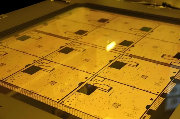
Rigid PCB copper weight refers to the mass of copper per unit area on the conductive layers, typically expressed in ounces per square foot (oz/ft2). This measurement equates to a specific thickness, where 1 oz/ft2 corresponds to approximately 35 micrometers of copper foil. Common weights include 0.5 oz/ft2, 1 oz/ft2, and 2 oz/ft2, with heavier options available for specialized needs. The copper foil is laminated onto the substrate during manufacturing, forming the traces and planes that carry signals and power. Thicker copper provides lower resistance paths, essential for high-performance rigid PCBs. Engineers must consider both nominal starting thickness and finished thickness after plating and etching processes.

In rigid PCBs, copper weight uniformity across layers affects overall board reliability. Standards such as IPC-6012E specify minimum finished copper thicknesses to ensure performance consistency. Deviations during fabrication can impact trace integrity, making precise specification vital.
Why Rigid PCB Copper Thickness Matters
Rigid PCB copper thickness influences multiple aspects of board performance, particularly in power electronics where heat generation is a concern. Thinner copper suits high-density signal routing but limits current handling, while thicker layers excel in power dissipation. Electrical engineers prioritize thickness to prevent overheating, which could lead to delamination or component failure. Impedance control also ties into copper weight, as variations alter signal propagation in multilayer stacks. Cost escalates with heavier copper due to material use and processing challenges. Ultimately, the right rigid PCB copper weight aligns electrical demands with mechanical stability.
Power delivery networks benefit from increased thickness, reducing voltage drops over long traces. In applications like motor drives or power supplies, inadequate thickness results in excessive I2R losses. Thermal management improves as thicker copper spreads heat more effectively across the board.
Technical Principles of Current Carrying Capacity
Rigid PCB current carrying capacity depends on trace width, copper thickness, and allowable temperature rise. According to IPC-2152, external traces handle higher currents than internal ones due to better convection cooling. Thicker copper lowers resistance, allowing greater amperage before reaching critical temperatures. Engineers calculate capacity using factors like ambient conditions and layer position. The standard provides charts correlating these variables for precise design.
Resistance in a trace follows R = ρL / A, where ρ is copper resistivity, L is length, and A is cross-sectional area. Doubling copper weight roughly doubles area, halving resistance and enabling higher currents. However, skin effect at high frequencies reduces effective thickness, favoring thinner foils for RF designs.
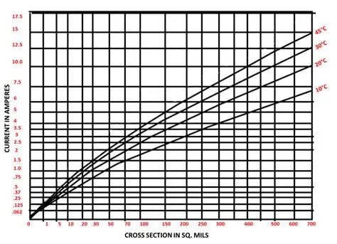
Power dissipation ties directly to current capacity, as P = I2R. Minimizing R through thicker copper reduces heat output for a given load. Yet, excessive thickness demands wider traces to avoid etching undercuts, impacting routing density.
Related Reading: Copper Weight (1oz vs. 2oz) and Current-Carrying Capacity
Power Dissipation in Rigid PCBs
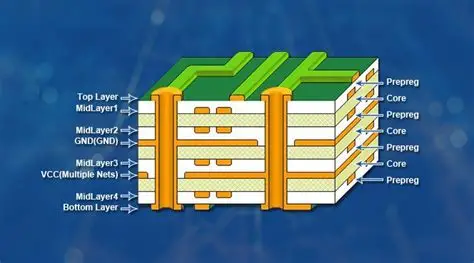
Rigid PCB power dissipation hinges on copper thickness to manage Joule heating effectively. Thicker foils offer lower thermal resistance, facilitating heat transfer to the environment or heatsinks. In high-power designs, multilayer boards with heavy copper planes act as thermal vias alternatives. Engineers model dissipation using finite element analysis alongside empirical data from standards. Layer stacking influences vertical heat flow, with outer layers dissipating better.
Copper's high thermal conductivity, around 400 W/m·K, makes it ideal for spreading localized heat from components. However, board thickness and material thermal properties modulate overall performance. Selecting rigid PCB copper weight optimizes the balance between electrical and thermal paths.
Factors Influencing Copper Weight Selection
Several factors guide rigid PCB copper thickness choices for electrical engineers. High-current paths, such as ground or power planes, require 2 oz/ft2 or more to handle amperage without excessive voltage drop. Signal integrity in high-speed designs favors 1 oz/ft2 for controlled impedance. Mechanical stress from thermal cycling increases with asymmetry in copper weights across layers, risking warpage.
Manufacturing tolerances narrow for heavier copper, as plating buildup affects fine features. Cost analysis weighs material expense against performance gains. Environmental factors like operating temperature range further dictate minimum thickness.
- 0.5 oz/ft2 — 18 μm — High-density signals
- 1.0 oz/ft2 — 35 μm — Standard power/signal
- 2.0 oz/ft2 — 70 μm — High current
- 3.0 oz/ft2 — 105 μm — Power electronics
This list summarizes common options, aiding quick reference in design reviews.
Best Practices for Selecting Rigid PCB Copper Thickness
Start by estimating peak currents using load analysis and apply IPC-2152 guidelines for trace sizing. Specify consistent weights across symmetric layers to minimize warpage per IPC-6012E requirements. Use via stitching for heavy copper planes to enhance current sharing. Simulate thermal profiles early to validate dissipation assumptions. Collaborate with fabricators on plating capabilities for non-standard weights.
Gradient copper weights, thinner inner layers and heavier outer, optimize for mixed-signal boards. Always factor in derating for harsh environments. Document rationale in design files for review.
Related Reading: Unlocking PCB Performance: The Secrets of Copper Weight Optimization
Manufacturing and Quality Considerations
Fabrication processes like panel plating add copper uniformly, but heavier starts demand precise etch control. IPC-6012E outlines acceptance criteria for finished thicknesses, ensuring reliability. Etch factor, the ratio of lateral to vertical etch, worsens with thick copper, necessitating wider traces. Inspection via cross-sectioning verifies compliance.
Solder mask and surface finishes interact with copper weight, affecting heat dissipation. Post-process annealing relieves stresses in heavy copper boards.
Conclusion
Selecting the right rigid PCB copper weight optimizes current carrying capacity and power dissipation for robust designs. Thicker copper enhances performance in power-intensive applications but requires careful tradeoffs in density and cost. Adhering to standards like IPC-2152 and IPC-6012E ensures compliance and reliability. Electrical engineers benefit from structured analysis of electrical, thermal, and mechanical factors. Thoughtful specification leads to efficient, long-lasting rigid PCBs tailored to application needs.
FAQs
Q1: What is the standard rigid PCB copper thickness for most applications?
A1: The 1 oz/ft2 weight, equating to 35 μm, serves as the default for many rigid PCBs balancing density and performance. It supports typical current carrying capacity needs while enabling fine-pitch routing. Heavier options like 2 oz/ft2 suit power sections. Always verify against IPC-2152 for specific calculations.
Q2: How does rigid PCB copper weight affect current carrying capacity?
A2: Higher copper weight increases cross-sectional area, reducing resistance and boosting rigid PCB current carrying capacity per IPC-2152 charts. External traces outperform internal ones due to cooling. Designers adjust width and thickness iteratively for target temperature rises, ensuring safe operation under load.
Q3: Why consider rigid PCB copper thickness for power dissipation?
A3: Thicker rigid PCB copper thickness lowers I2R losses, improving power dissipation by minimizing heat generation. It also aids lateral heat spreading to vias or edges. In multilayer stacks, balanced weights prevent hotspots. Simulations complement standard guidelines for validation.
Q4: Can rigid PCB copper weight vary between layers?
A4: Yes, asymmetric weights are common, with heavier outer layers for power and thinner inners for signals. This enhances overall rigid PCB current carrying capacity while controlling impedance. IPC-6012E addresses warpage risks from imbalances. Specify clearly in stack-up documentation.
References
[IPC-2152 — Standard for Determining Current Carrying Capacity in Printed Board Design. IPC, 2009]
[IPC-6012E — Qualification and Performance Specification for Rigid Printed Boards. IPC, 2015]
[IPC-A-600K — Acceptability of Printed Boards. IPC, 2020]