 ALLPCB


Introduction
Precision microvia drilling plays a pivotal role in fabricating high-density PCBs, enabling the tight interconnects required for advanced electronics. As devices shrink and component pitches decrease, engineers rely on microvias to maximize routing density while preserving signal integrity. Laser drilling microvias offers unmatched accuracy for via sizes below 150 microns, surpassing traditional mechanical methods in finesse and repeatability. This technique addresses the challenges of multilayer stackups in high-density PCBs, where every micron counts toward performance and reliability. Factory processes emphasize controlled parameters to ensure vias meet rigorous quality thresholds from drilling through plating.
What Are Microvias and Why Do They Matter in High-Density PCBs?
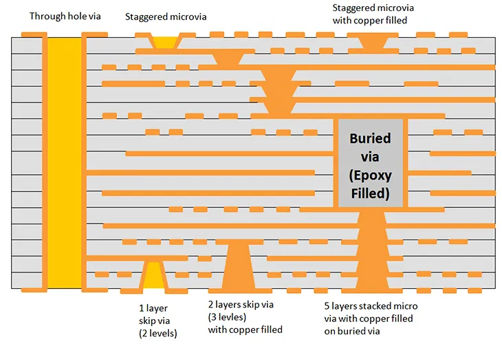
Microvias represent a class of blind or buried vias with diameters typically at or below 150 microns, designed to connect adjacent layers without penetrating the entire board. In high-density PCBs, these vias facilitate finer trace spacing and higher component density, essential for applications like smartphones and medical devices. Unlike standard through-holes, microvias minimize board real estate usage, allowing more layers for signals and power distribution. Their small via size reduces stub lengths, which directly enhances signal integrity by lowering inductance and reflections at high frequencies. From a manufacturing standpoint, microvias demand specialized processes to achieve consistent yields, as imperfections can propagate failures during thermal cycling or vibration.
The relevance of microvia drilling intensifies with the shift to HDI structures, where build-ups incorporate stacked or staggered microvias for ultra-fine interconnects. Engineers must consider via size when planning layer counts, as smaller diameters enable tighter pitches but complicate plating uniformity. Signal integrity benefits emerge from shorter via paths, reducing crosstalk and insertion loss in gigahertz signals. Factory insights reveal that high-density PCBs without precise microvias often face routing congestion, forcing compromises in design rules.
Technical Principles of Laser Drilling Microvias
Laser drilling microvias employs pulsed laser beams to ablate material selectively, creating precise holes in dielectrics and copper foils. Ultraviolet lasers excel at vaporizing both copper and resin simultaneously, producing straight-sided vias with minimal taper. Carbon dioxide lasers, conversely, target organic dielectrics effectively after copper etching, suiting sequential lamination processes. The ablation mechanism relies on photon energy breaking molecular bonds, ejecting debris as plasma without mechanical stress. This non-contact method achieves via sizes from 50 to 150 microns, far smaller than mechanical drilling limits.
Key parameters include pulse duration, repetition rate, and fluence, which control hole depth and sidewall quality. Aspect ratios typically stay at or below 1:1, with 0.75:1 preferred for optimal plating throw. In high-density PCBs, via size tolerances tighten to plus or minus 10 microns, demanding fiducial alignment for multilayer registration. Signal integrity ties into these principles, as uniform via geometry minimizes impedance discontinuities. Factories calibrate lasers per panel to compensate for material variations, ensuring repeatability across production runs.
Thermal effects during drilling influence via reliability, with excessive heat causing resin charring or copper smear. Advanced systems use trepanning or helical scanning to distribute energy evenly, reducing heat-affected zones. Post-drill desmear removes residue, preparing surfaces for electroless copper deposition. These steps align with industry expectations for clean, conical-free vias in high-density PCBs.
Challenges in Precision Microvia Drilling for High-Density PCBs
Achieving precision in microvia drilling encounters hurdles like registration accuracy across thin dielectrics, where misalignment exceeds 25 microns and causes open circuits. Debris from ablation can redeposit on walls, compromising plating adhesion and leading to voids. In stacked microvias, cumulative tolerances amplify risks, potentially cracking under reflow stresses. Via size variations from material inconsistencies further degrade signal integrity through uneven impedance profiles. Manufacturers mitigate these by selecting laser-drillable resins with low ablation thresholds.
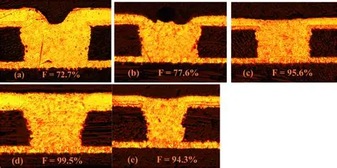
Reliability testing per IPC-6016 reveals that microvias must withstand thermal shock without separation, emphasizing plating thickness uniformity. High-density PCBs amplify these issues, as dense via fields strain panel handling and inspection. Taper control proves critical, with excessive coning hindering bottom copper coverage. Factories implement automated optical inspection to flag anomalies early, preserving yield.
Best Practices for Microvia Drilling in High-Density PCBs
Start with material selection favoring laser-ablatable dielectrics, such as those with uniform glass transition temperatures for consistent ablation. Optimize drilling sequences by grouping vias by layer, minimizing panel movement and enhancing throughput. Maintain aspect ratios at 0.75:1 or less to ensure plating reaches via bottoms without thinning, as guided by IPC-2226. Post-drill plasma cleaning removes organics thoroughly, followed by permanganate desmear for residue-free walls. These practices directly support signal integrity in high-density PCBs by delivering reliable interconnects.
Via size planning integrates with design rules, targeting 75 to 100 microns for most HDI layers to balance density and manufacturability. Factories employ fiducials and optical alignment for sub-20-micron registration, crucial in buildup processes. Sequential lamination allows staggered microvias, distributing stress and improving thermal performance. Plating follows with pulse reverse electroplating to build 15 to 20 microns of copper uniformly. Inspection via cross-sectioning verifies geometry before fill or cap.
For high-volume runs, calibrate laser power dynamically based on feedback from test vias, compensating for panel warp. Avoid overstacking beyond four microvias without stagger to prevent reliability failures. These factory-driven approaches yield high first-pass rates, essential for cost control.
Optimizing Via Size for Signal Integrity in High-Density PCBs
Smaller via sizes in microvia drilling reduce parasitic inductance, critical for high-speed signals where stubs cause ringing. In high-density PCBs, microvias shorten return paths, lowering loop inductance and improving eye diagrams. Engineers model via transitions using field solvers to predict discontinuities, adjusting pad sizes accordingly. Laser-drilled walls provide smoother transitions than mechanical vias, minimizing reflections. Factory data confirms that via sizes under 100 microns enhance crosstalk isolation in dense routing.
Impedance control ties via size to trace width, with microvias enabling 50-ohm lines at finer pitches. Stacked configurations demand careful sequencing to avoid cumulative losses. Signal integrity simulations guide via placement away from aggressors. These optimizations ensure compliance with performance specs in demanding applications.
Troubleshooting Common Issues in Microvia Drilling
When vias exhibit dog-boning, inspect desmear efficacy and plating bath chemistry for bottom-heavy deposition. Cracking in stacked microvias often stems from CTE mismatch, resolved by symmetric stackups and low-stress fills. Poor registration signals fiducial wear, addressed via panel-level corrections. Debris-induced shorts require enhanced vacuum extraction during drilling. Factories log parameters to trace root causes, iterating processes swiftly.
Conclusion
Precision microvia drilling unlocks the potential of high-density PCBs through exact via sizes and superior signal integrity. Laser drilling microvias excels in creating reliable interconnects for compact designs, guided by proven manufacturing practices. Adhering to aspect ratio limits and rigorous inspection ensures long-term performance. Electric engineers benefit from these insights to streamline designs for production. Ultimately, mastering this process drives innovation in electronics density and efficiency.
FAQs
Q1: What is the typical via size range for microvia drilling in high-density PCBs?
A1: Microvia drilling targets diameters from 50 to 150 microns, with 75 to 100 microns common for optimal density. This via size balances routing freedom and plating reliability in HDI structures. Factories prioritize these dimensions to maintain yields, as smaller sizes risk incomplete fills while larger ones waste space. Signal integrity improves with precise sizing to minimize discontinuities.
Q2: How does laser drilling microvias impact signal integrity in high-density PCBs?
A2: Laser drilling microvias reduces via stub lengths and inductance, preserving waveform integrity at high frequencies. Cleaner walls from ablation lower insertion loss compared to mechanical vias. In high-density PCBs, this enables dense routing without excessive crosstalk. Manufacturers verify through time-domain reflectometry for consistent performance.
Q3: What aspect ratios are recommended for microvias per industry standards?
A3: IPC-2226 recommends a maximum 1:1 aspect ratio for microvias, preferring 0.75:1 for uniform plating. This ensures copper coverage in high-density PCBs during electroless and electrolytic steps. Exceeding these risks voids or cracks under thermal stress. Factories enforce these in design reviews for reliability.
Q4: Why choose laser over mechanical drilling for microvias in high-density PCBs?
A4: Laser drilling achieves sub-150-micron via sizes unattainable mechanically, with better registration in thin dielectrics. It avoids bit wear and smear, suiting HDI buildup. Mechanical suits larger holes but falters in precision for microvias. This choice enhances signal integrity through superior geometry control.


