 ALLPCB


Introduction
Aerospace and defense applications push electronic components to their limits with conditions like rapid thermal cycling, high radiation exposure, intense vibrations, and mechanical shocks. Standard organic substrates such as FR-4 fail quickly under these stresses due to thermal degradation, delamination, or electrical breakdown. Ceramic PCBs emerge as the preferred choice for ceramic PCB aerospace and ceramic PCB defense systems because they maintain structural integrity and electrical performance in extreme environments. These boards leverage inorganic materials that resist degradation far better than polymers. Engineers designing for satellites, avionics, radar arrays, or missile guidance must prioritize such solutions to ensure mission reliability. This article explores the properties, mechanisms, and best practices that make ceramic PCBs indispensable.
Understanding Ceramic PCBs and Their Relevance
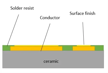
Ceramic PCBs use substrates like alumina or aluminum nitride, processed via methods such as direct bonded copper or thick-film printing. Unlike laminate-based boards, they offer inherent advantages in thermal dissipation and dimensional stability. In aerospace and defense, where failure rates must approach zero, these boards handle power densities that would overwhelm conventional PCBs. Extreme environment PCBs demand materials that align with silicon or gallium nitride components, minimizing stress during temperature swings. Ceramic PCB defense applications include high-frequency radar modules and propulsion controls, while ceramic PCB aerospace uses span satellite payloads and engine monitors. Factory insights reveal that selecting the right ceramic type directly impacts long-term field performance.
The relevance stems from mission-critical needs: a single board failure in space or combat can lead to total system loss. Ceramics provide a hermetic barrier against moisture and contaminants, essential in vacuum or corrosive atmospheres. Their non-organic composition avoids outgassing, a common issue in space that fouls optics or sensors. Engineers appreciate how these boards support dense interconnects without compromising signal integrity. Overall, ceramic PCBs bridge the gap between component-level reliability and system-level endurance.
Core Properties Enabling Performance in Extreme Conditions
Superior Thermal Conductivity and Management
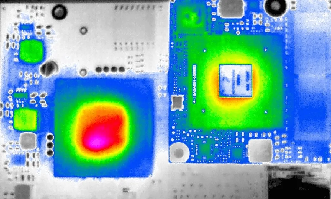
Ceramic PCBs excel in high-temperature PCB scenarios due to their thermal conductivity, often exceeding that of metals in thin layers. Heat from power amplifiers or converters dissipates rapidly, preventing hotspots that cause solder joint fatigue or component burnout. In turbine engines or re-entry vehicles, temperatures fluctuate wildly, but ceramics maintain low thermal resistance paths. This property reduces junction temperatures in attached semiconductors, extending operational life. Factory processes ensure uniform metallization for optimal heat spreading. Engineers model these boards with finite element analysis to predict gradients accurately.
The coefficient of thermal expansion closely matches semiconductors, around 4 to 7 ppm per degree Celsius for alumina, curbing warpage during assembly or service. Thermal cycling tests simulate aerospace profiles, validating stability over thousands of cycles. Without this match, micro-cracks propagate under vibration, leading to intermittent failures. Ceramic substrates enable direct bonding of high-power devices, eliminating thermal interface materials that add resistance.
Radiation Resistance and Electrical Stability
Radiation-resistant PCB demands arise in space from cosmic rays and solar flares, which degrade organic dielectrics through ionization and charge buildup. Ceramics resist this by lacking mobile ions or polymers that trap radiation-induced charges. Their high dielectric strength, often over 20 kV per millimeter, prevents arcing in high-voltage circuits. In defense satellites or nuclear-hardened systems, this translates to sustained performance without parametric drift. Electrical insulation remains consistent across wide humidity ranges, unlike hygroscopic laminates.
High-frequency signals in radar or communication links benefit from low dielectric loss tangents in ceramics. Radiation exposure hardens the material further, unlike organics that embrittle. Factory qualification involves accelerated radiation simulations to confirm latch-up immunity. These properties make ceramic PCBs vital for RF front-ends in contested environments.
Mechanical Robustness Against Shock and Vibration
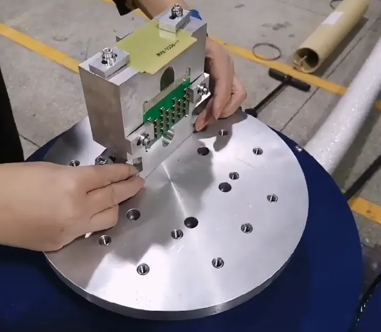
Extreme vibrations from rocket launches or jet maneuvers test board integrity, where ceramics' high Young's modulus resists flexing. They withstand accelerations over 100 g without fracturing when designed with proper thickness and support. Low porosity after firing ensures no microcracks under cyclic loading. In defense munitions, this durability supports guidance electronics through high-g impacts. Vibration damping layers can integrate without sacrificing thermal paths.
Standards like IPC-6012 guide qualification for such mechanical stresses, ensuring trace adhesion and via reliability. IPC-A-600 defines acceptability criteria for surface finish and plating integrity post-stress.
Design and Manufacturing Best Practices
Designing ceramic PCBs starts with material selection based on thermal needs: alumina for cost-effective insulation, aluminum nitride for maximum conductivity. Layouts minimize vias in high-heat zones, favoring embedded traces. Copper thickness up to 300 microns supports current densities over 10 A per mm squared without excessive rise. Simulation tools predict warpage from CTE mismatches early. Factory-driven insights emphasize cofiring for multilayers to achieve hermetic seals.
Manufacturing involves precise laser drilling for blind vias, as mechanical methods risk chipping. Thick-film pastes fire at controlled ramps to avoid substrate cracks. Surface metallization uses sputtering for adhesion, tested per IPC-6012 for peel strength. Post-processing includes helium leak checks for space-grade seals. Engineers specify edge plating for mechanical clamping in housings.
Assembly challenges include higher reflow temperatures, addressed by low-alpha solders to minimize radiation effects. JEDEC J-STD-020 guidelines adapt for moisture sensitivity, though ceramics absorb little. Gold wire bonding or flip-chip ensures low-resistance connections. Quality control scans for voids using X-ray, aligning with factory standards for zero-defect goals.
Real-World Applications and Insights
In satellite power supplies, ceramic PCBs manage DC-DC converters under solar radiation, dissipating kilowatts without derating. Avionics computers use them for processor boards enduring -55 to 125 degrees Celsius cycles. Radar transmitters leverage the boards' low loss for phased arrays scanning at gigahertz frequencies. Missile seekers integrate high-temperature PCBs near warheads, surviving pyrotechnic shocks.
Troubleshooting common issues involves thermal profiling during prototyping. Warpage appears from asymmetric copper, corrected by balanced patterning. Radiation testing reveals soft errors in unsupported logic, mitigated by triple modular redundancy on ceramics. Factory data shows failure rates below 1 ppm after qualification.
Conclusion
Ceramic PCBs stand out in aerospace and defense for their unmatched resilience in extreme environments, from scorching re-entry heat to cosmic radiation. Their thermal prowess, mechanical strength, and electrical purity enable compact, reliable designs that organic alternatives cannot match. Electrical engineers benefit from factory-aligned processes that deliver consistent performance. Prioritizing these boards reduces risks in high-stakes missions. Future advancements will further integrate them into hybrid modules, solidifying their role.
FAQs
Q1: Why are ceramic PCBs preferred for ceramic PCB aerospace applications?
A1: Ceramic PCBs offer superior thermal conductivity and low CTE matching silicon, essential for thermal cycling in satellites and avionics. They resist radiation-induced degradation, maintaining signal integrity in space. Factory processes ensure hermetic sealing against vacuum outgassing. This combination supports high-power density without failure, aligning with IPC Class 3 requirements for reliability.
Q2: How do ceramic PCBs handle high-temperature PCB demands in defense?
A2: In defense radar and propulsion, ceramic substrates operate stably at elevated temperatures where FR-4 delaminates. High dielectric strength prevents breakdowns under voltage spikes. Vibration resistance from high modulus protects traces during shocks. Manufacturing adapts thick-film techniques for durable metallization. Engineers gain confidence from standardized qualification like IPC-A-600.
Q3: What makes ceramic PCBs radiation-resistant PCB choices for extreme environments?
A3: Ceramics lack polymers that trap radiation charges, avoiding latch-up in electronics. Their inorganic structure endures ionizing doses from flares or reactors. Low loss tangents preserve RF performance post-exposure. Factory radiation simulations validate this for space-grade use. JEDEC guidelines aid component integration on these stable platforms.
Q4: Are there best practices for designing extreme environment PCBs with ceramics?
A4: Select substrate by thermal needs, simulate warpage, and balance copper distribution. Use direct bond copper for heat paths and laser vias for density. Qualify per IPC-6012 for mechanical stress. Factory insights stress precise firing to minimize porosity. This ensures reliability in aerospace vibrations and temps.





