 ALLPCB


Introduction
In high-speed PCB manufacturing, signal integrity challenges arise from via stubs in multilayer boards. PCB back drilling, a controlled depth drilling technique, addresses this by removing excess copper from through-hole vias. This process enhances electrical performance for electrical engineers designing circuits operating at multi-gigabit speeds. As part of the PCB manufacturing process, CNC back drilling requires precision to maintain board integrity. This guide provides a PCB back drilling tutorial focused on practical implementation using CNC machines. Engineers can follow these steps to optimize via drilling techniques and achieve reliable controlled depth drilling.
What Is PCB Back Drilling and Why It Matters
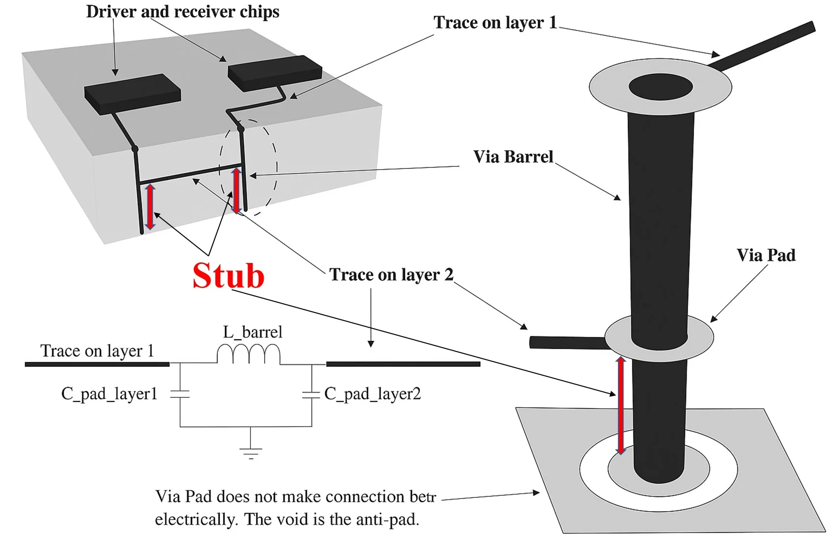
PCB back drilling removes the unused portion of a plated through-hole via, known as the stub, which extends beyond the last connected layer. These stubs act as impedance discontinuities, causing signal reflections, insertion loss, and crosstalk in high-frequency applications. By shortening the via to just above the target layer, back drilling improves return loss and eye diagram quality. This technique matters in modern PCBs where data rates exceed 3 Gbps, as stubs longer than one-tenth of the signal wavelength degrade performance. Factory processes integrate back drilling post-plating to support dense, high-layer-count designs. Electrical engineers rely on it to meet stringent signal integrity requirements without redesigning the stackup.
In the PCB manufacturing process, back drilling distinguishes standard through-vias from optimized ones for critical nets. It allows cost-effective use of through-holes instead of blind or buried vias in many cases. Compliance with standards like IPC-6012 ensures the drilled depth meets qualification criteria. Ultimately, this method balances performance and manufacturability for complex boards.
Technical Principles of CNC Back Drilling
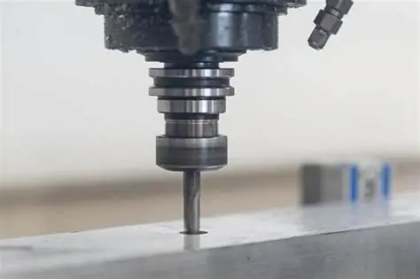
CNC back drilling uses computer numerical control machines with Z-axis depth sensing to perform precise excavation. The process starts after initial via drilling and electroplating, targeting the copper barrel from the opposite side. A larger drill bit, typically oversized by 8 to 10 mils relative to the original via diameter, cleanly removes the stub while leaving a minimal residual length. Depth control relies on optical registration, stackup thickness data, and feedback systems to avoid breakthrough into active layers. This controlled depth drilling guide emphasizes Z-axis accuracy, often within 2 to 10 mils tolerance depending on board thickness.
Signal improvement stems from reducing stub length, which minimizes parasitic capacitance and inductance. Shorter stubs lower resonance frequencies that interfere with harmonics. Factory-driven insights highlight the need for accurate CAM programming to map via locations per net class. Material properties like FR-4 dielectric constant influence drilling parameters, such as spindle speeds from 40,000 to 100,000 RPM and controlled feed rates. Proper chip load prevents bit breakage and burrs. These principles ensure via drilling techniques align with high-reliability production.
Step-by-Step Guide to PCB Back Drilling with CNC Machines
Step 1: Design Preparation and Via Identification
Begin by identifying high-speed vias in the PCB layout that require stub removal. Review the stackup to determine the target depth for each via, ensuring clearance to inner layer traces exceeds 10 mils. Specify backdrill requirements in fabrication notes, including oversize diameter and residual stub length. Generate separate drill files for backdrilling, listing X-Y coordinates, depths, and bit sizes. Electrical engineers should simulate signal integrity pre- and post-backdrill to validate benefits. This preparation integrates seamlessly into the PCB manufacturing process.
Step 2: CAM Programming for CNC
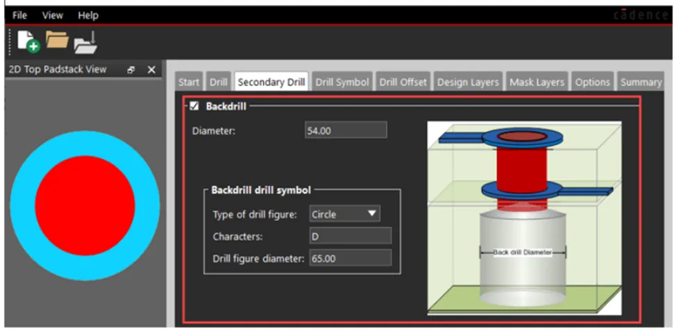
Load the Gerber and drill files into CAM software to create the backdrill program. Define Z-depth per via group, accounting for panel thickness variations and plating buildup. Set backdrill bit diameter 8 to 10 mils larger than the primary via to fully excise the copper barrel. Program entry and exit points to minimize breakout on outer layers. Include verification holes as required by IPC-6012 for depth validation. Optimize tool paths to reduce cycle time while maintaining registration accuracy.
Step 3: CNC Machine Setup
Secure the plated PCB panel on the CNC drill bed using registration pins for alignment. Calibrate the Z-axis with a depth sensor or optical probe to measure stackup precisely. Select rigid carbide backdrill bits suited for the material, installing them in the spindle. Input parameters like spindle speed around 60,000 RPM and feed rate for optimal chip evacuation. Perform a dry run to verify alignment against fiducials. Factory protocols include panel inspection for warpage before setup.
Step 4: Execute Controlled Depth Drilling
Initiate drilling from the opposite side of the intended signal path. The CNC advances the bit to the programmed depth, stopping short of the target pad by 5 to 10 mils. Monitor real-time Z-feedback to adjust for any deviations. Multiple passes may apply for thicker boards to ensure clean stub removal. Coolant or air blast clears debris during operation. This CNC back drilling step demands constant oversight for tolerance adherence.
Step 5: Post-Drilling Inspection and Cleaning
After drilling, inspect depths using cross-sectioning on coupons or X-ray for production panels. Verify stub lengths and check for over-drill or under-drill via automated visual inspection. Clean holes with desmear or plasma to remove residue. Measure backdrill clearances to adjacent features. IPC-A-600 provides acceptability criteria for drilled features. Proceed only after confirming no damage to inner layers.
Step 6: Integration into Full Manufacturing Flow
Route backdrilled panels to solder mask application, ensuring openings accommodate the enlarged entrance. Final plating may fill any dimples from the process. Bake-out removes moisture before assembly. Track yield data to refine future runs. This completes the via drilling techniques phase, readying boards for high-speed use.
Best Practices for CNC Back Drilling
Maintain clearances of at least 10 mils between backdrills and planes or traces to prevent shorts. Limit backdrilling to nets above 3 Gbps where stubs impact performance most. Use consistent stackup data from suppliers for accurate depth programming. Employ high-precision CNC with sub-5 mil Z-tolerance for thick boards over 4 mm. Sequence backdrills by depth to optimize tooling changes. Regular bit inspection prevents defects.
Adhere to IPC-2221 guidelines for via design to minimize initial stub issues. Simulate drilling forces based on material to set feeds preventing delamination. Panel size affects warpage, so use fixtures for stability. Document all parameters for repeatability. These practices elevate PCB back drilling tutorial outcomes in production.
Common Challenges and Troubleshooting
Over-drilling risks breakthrough, detected by continuity tests on verification nets. Solution: Tighten Z-control and add safety margins. Burrs or rough walls from improper speeds cause plating voids; adjust RPM upward and feeds downward. Misregistration from panel shift requires better pinning. Stub remnants longer than spec degrade signals; verify with time-domain reflectometry. Warpage in thick multilayers demands flatness checks pre-drill.
Under-drilling leaves excessive stubs, addressed by process tuning and coupon validation. Debris contamination post-drill affects yield; enhance cleaning steps. These factory-driven insights help electrical engineers troubleshoot effectively.
Conclusion
PCB back drilling with CNC machines optimizes via performance in high-speed designs through precise stub removal. This controlled depth drilling guide outlines steps from design to inspection, emphasizing accuracy and standards compliance. Electrical engineers benefit from reduced signal degradation and reliable manufacturing. Integrating best practices ensures consistent results in the PCB manufacturing process. Adopt these via drilling techniques to enhance board quality.
FAQs
Q1: What is the typical oversize for a backdrill bit in PCB back drilling tutorial?
A1: In CNC back drilling, the backdrill bit diameter is usually 8 to 10 mils larger than the original via drill size. This ensures complete removal of the copper stub without excessive enlargement. Proper oversize prevents residue while maintaining structural integrity. Factory processes confirm this via test coupons for each job.
Q2: How does CNC back drilling improve signal integrity in the PCB manufacturing process?
A2: CNC back drilling shortens via stubs, reducing reflections and insertion loss for high-speed signals. Shorter stubs minimize impedance mismatches and crosstalk. This technique supports data rates over 3 Gbps effectively. Engineers verify improvements through simulations and measurements.
Q3: What tolerances apply to controlled depth drilling guide in backdrilling?
A3: Depth tolerances typically range from ±2 to 10 mils, based on board thickness and equipment precision. Z-axis control maintains accuracy to avoid layer damage. Verification holes per IPC standards confirm compliance. Consistent stackup data aids tolerance achievement.
Q4: When should electrical engineers specify backdrilling in via drilling techniques?
A4: Specify backdrilling for through-vias on nets exceeding 3 Gbps or with stubs longer than one-tenth wavelength. It suits multilayer boards where blind vias increase cost. Design clearances early to enable manufacturability. This optimizes the PCB manufacturing process.
References
IPC-6012E — Qualification and Performance Specification for Rigid Printed Boards. IPC, 2017
IPC-2221B — Generic Standard on Printed Board Design. IPC, 2012
IPC-A-600K — Acceptability of Printed Boards. IPC, 2020


