 ALLPCB


Why VR Headset PCB Power Consumption Matters
Power consumption in VR headset PCBs determines how long a device can operate on a single charge. High draw from graphics processing units and high resolution displays accelerates battery depletion and generates excess heat. This heat can affect component reliability and user comfort when the headset rests against the face. Industry professionals recognize that optimized PCB designs extend battery life while preserving the performance required for smooth tracking and rendering. Reduced power use also supports smaller battery packs, which helps lower overall device mass and improves ergonomics for prolonged wear.
Technical Principles of Power Management in VR Headset PCBs
VR headset PCBs distribute power through multiple voltage domains to serve diverse components such as application processors, micro displays, inertial measurement units, and communication radios. Each domain requires stable voltage regulation to avoid noise that could degrade sensor accuracy or display uniformity. Engineers apply techniques such as dynamic voltage and frequency scaling to adjust supply levels based on workload, thereby cutting unnecessary energy use during lighter tasks. Board layout plays a critical role because trace resistance and via placement influence resistive losses that convert electrical energy into heat. Careful partitioning of analog and digital sections prevents crosstalk that might force higher operating margins and increased consumption. Thermal vias and copper pours help conduct heat away from power intensive areas, maintaining component temperatures within acceptable ranges for reliable operation.
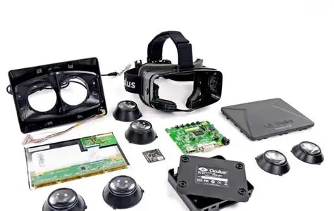
Component selection further shapes overall efficiency. Low quiescent current regulators and high efficiency switching converters reduce standby losses that accumulate over time. Display drivers and backlight circuits often account for a substantial share of total draw, so pulse width modulation dimming combined with efficient LED arrays helps lower this contribution. Sensor fusion algorithms running on the processor can enter low power states when motion tracking is not required, allowing the PCB to throttle activity intelligently. These mechanisms work together to balance performance demands with energy conservation across varying usage scenarios.
Practical Solutions and Best Practices for Low Power PCB Design
Design teams begin by mapping power budgets for each functional block early in the development cycle. This mapping identifies high consumption areas and guides decisions on supply architecture and component ratings. Multi layer PCBs with dedicated power and ground planes minimize impedance and improve current return paths, which reduces voltage drops and associated losses. Placement of decoupling capacitors close to integrated circuits suppresses transient currents that would otherwise increase average power draw.
Engineers also evaluate the use of advanced packaging options that shorten interconnect lengths and lower parasitic capacitance. Board level simulation of power integrity helps verify that voltage rails remain stable under peak loads without excessive oversizing of regulators. Compliance with relevant manufacturing standards supports consistent quality in these complex assemblies.
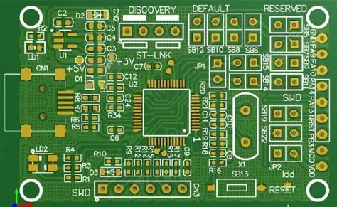
Material choices influence both electrical and thermal performance. Substrates with appropriate dielectric properties support fine line routing needed for dense interconnects while managing signal integrity at high speeds. Thermal interface materials between the PCB and heat spreading elements aid in dissipating energy from power semiconductors. Iterative testing of prototypes under representative workloads validates that design choices deliver measurable reductions in consumption without compromising functionality.
Conclusion
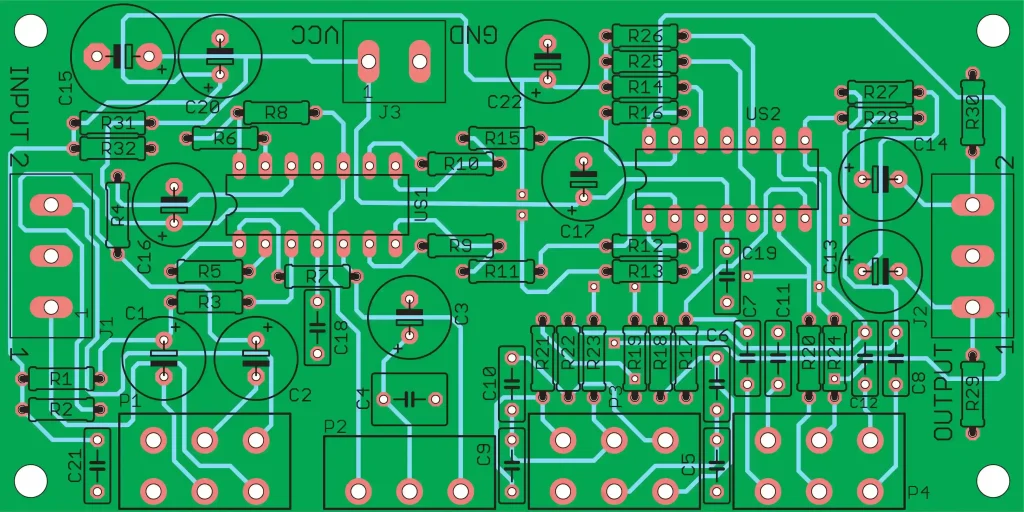
Optimizing VR headset PCB power consumption requires coordinated attention to architecture, layout, component selection, and thermal management. These efforts yield devices that operate longer on each charge while maintaining the performance expected in metaverse applications. Structured engineering practices ensure that power efficiency improvements integrate reliably into production volumes.
FAQs
Q1: How does VR headset PCB power consumption affect battery life?
A1: VR headset PCB power consumption directly determines runtime because the board supplies energy to processors, displays, and sensors. Lower consumption through efficient regulation and layout allows the same battery capacity to support longer sessions. Engineers balance these reductions against performance needs to avoid compromising immersion or tracking accuracy.
Q2: What are key techniques in low power PCB design for VR headsets?
A2: Low power PCB design for VR headsets involves dynamic voltage scaling, efficient converter selection, and optimized trace routing to cut resistive losses. Partitioning power domains and placing decoupling components strategically further reduce waste. These methods collectively extend operation while preserving the high speed signaling required for real time graphics and motion data.
Q3: Why is power management important in VR headset applications?
A3: Power management in VR headset applications prevents rapid battery drain and excessive heat buildup that could limit comfortable use. Effective management at the PCB level supports compact form factors and reliable component operation over repeated charge cycles. It enables the sustained performance needed for interactive metaverse environments without frequent recharging interruptions.
Q4: How can engineers improve efficient PCB VR designs?
A4: Engineers improve efficient PCB VR designs by conducting early power budgeting and using simulation tools to validate layout choices. Attention to ground plane integrity and thermal paths helps maintain stable operation at reduced energy levels. Iterative refinement based on measured consumption data ensures designs meet both performance and endurance targets.
References
IPC-6012E — Qualification and Performance Specification for Rigid Printed Boards. IPC, 2017
JEDEC J-STD-020E — Moisture/Reflow Sensitivity Classification. JEDEC, 2014
ISO 9001:2015 — Quality Management Systems. ISO, 2015





