 ALLPCB


Introduction
Engineers designing printed circuit boards face constant pressure to balance performance, reliability, and manufacturability. A PCB copper weight calculator emerges as an essential tool in this process, enabling precise determination of copper foil thickness and its impact on overall board functionality. This online copper weight calculator simplifies conversions between ounces per square foot and microns, while integrating features like PCB trace width calculator and PCB current carrying capacity calculator functionalities. By inputting parameters such as current load, temperature rise allowance, and layer position, engineers obtain optimized trace dimensions that prevent overheating and ensure signal integrity. Adhering to established guidelines like IPC-2152 helps mitigate risks in high-density designs. Ultimately, such tools empower electric engineers to make data-driven decisions early in the design cycle.
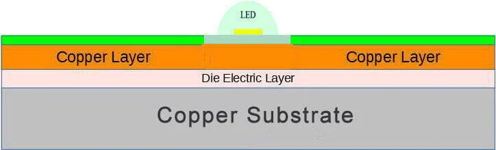
What Is PCB Copper Weight and Why It Matters
PCB copper weight refers to the mass of copper foil per unit area, typically expressed in ounces per square foot. This metric directly correlates to the physical thickness of the copper layer, with 1 ounce equating to approximately 35 microns nominally before processing. Engineers select copper weights ranging from 0.5 to 3 ounces based on power requirements, thermal management needs, and space constraints. Lighter weights suit high-frequency signals where thin traces minimize inductance, whereas heavier weights support high-current paths in power electronics. Misjudging copper weight can lead to excessive temperature rises, electromigration, or delamination under thermal stress. In practice, accurate calculation ensures compliance with performance specs and extends board lifespan.
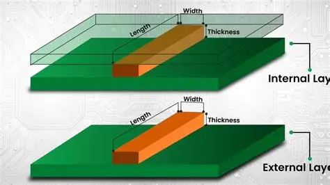
The relevance intensifies in multilayer boards, where internal layers demand different considerations than external ones due to heat dissipation differences. An online copper weight calculator proves invaluable here, allowing quick assessments of total copper mass for mechanical stability or shipping weight estimates. For electric engineers, integrating this with PCB current carrying capacity calculations prevents undersized traces that could fail under load. Industry data underscores that improper sizing contributes to a significant portion of field failures in power supplies and motor controls. Thus, mastering copper weight selection optimizes both electrical and thermal performance.
Technical Principles Behind Copper Weight Calculations
Copper weight calculations stem from fundamental material properties and empirical data compiled in standards. The cross-sectional area of a trace, determined by width and thickness, dictates its resistance and heat generation via I2R losses. IPC-2152 provides comprehensive charts and equations modeling temperature rise as a function of current, copper weight, ambient conditions, and board thickness. Unlike earlier approximations, this standard accounts for variables like external versus internal traces and plating thickness, offering more conservative yet realistic predictions. Engineers input these into a PCB trace width calculator to solve for optimal dimensions, ensuring the trace temperature stays within safe limits, typically 10 to 20 degrees Celsius above ambient.
Heat dissipation mechanisms further influence outcomes, including conduction to adjacent planes, convection to air, and radiation. Thicker copper, corresponding to higher weights, reduces resistance but increases lateral heat spreading, which IPC-2152 quantifies through test-derived curves. For instance, doubling copper weight from 1 to 2 ounces roughly halves the required trace width for the same current, though diminishing returns apply at extremes. Online copper weight calculators also handle conversions precisely, using density of copper at 8.96 grams per cubic centimeter to translate ounces to microns accurately. Understanding these principles allows engineers to iterate designs logically, avoiding overdesign that wastes material or underdesign that risks reliability.
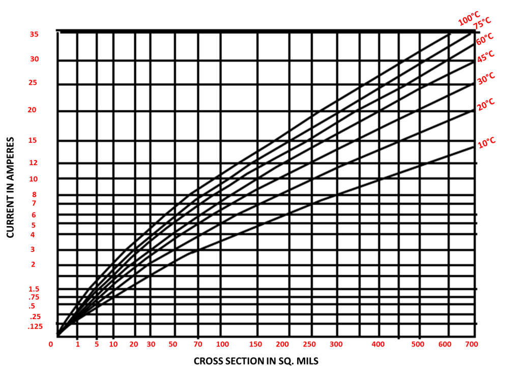
Previous guidelines in IPC-2221 offered simpler nomographs but underestimated risks for certain configurations, prompting the shift to IPC-2152. Modern calculators emulate these updated models, incorporating factors like board cross-section and fill factor for planes. This evolution reflects broader testing on actual boards rather than isolated traces, providing structured guidance for complex assemblies.
Practical Solutions and Best Practices for Using PCB Calculators
Electric engineers leverage PCB copper weight calculators during schematic capture and layout phases for proactive sizing. Start by defining requirements: maximum current, allowable temperature rise, and layer stackup. A PCB current carrying capacity calculator then outputs minimum trace widths, factoring in selected copper weight. For external traces, wider options suffice due to better cooling, while internal traces often require 1.5 to 2 times the width. Always apply a safety margin of 20 to 50 percent beyond calculated values to account for manufacturing tolerances and aging effects.
Best practices include verifying calculator outputs against simulation tools for dynamic loads. Select copper weights judiciously: 1 ounce for most signals, 2 ounces for moderate power, and heavier for high-current rails. Use the online copper weight calculator to estimate total board copper for warpage analysis, as imbalance between layers can cause bowing. In high-reliability applications, reference IPC-6012 for finished copper thickness minima post-plating. Document assumptions in design reviews to facilitate team alignment and future revisions.
Troubleshooting common issues enhances calculator efficacy. If traces overheat in prototypes, check for unaccounted vias or plane stitching that alters heat paths. For dense layouts, employ thermal reliefs and wider pours. Integrating a PCB trace width calculator into workflows streamlines iterations, reducing spin cycles. Regularly update to latest standard-based algorithms ensures ongoing accuracy.
Case Study: Optimizing High-Current Power Distribution
Consider a power distribution module for an industrial inverter, handling 50 amperes per phase across multilayer boards. Initial designs using 1-ounce copper resulted in excessive widths encroaching on signal routing. Switching to a PCB current carrying capacity calculator compliant with IPC-2152 revealed that 2-ounce external layers halved trace widths while maintaining 10-degree rise limits. Engineers adjusted internal layers to 1 ounce with additional stitching vias for heat extraction.
This adjustment not only freed space for control signals but also improved impedance matching. Total copper weight calculations confirmed mechanical stability, preventing warpage in reflow. Post-build thermal imaging validated predictions, with peaks aligning closely to modeled values. Such structured application demonstrates how tools transform constraints into efficient solutions.
Conclusion
PCB copper weight calculators stand as indispensable aids for electric engineers, bridging theory and practice in trace sizing and thermal management. By harnessing PCB trace width calculators and PCB current carrying capacity features, designers achieve reliable, compact boards aligned with IPC standards. Key takeaways include prioritizing IPC-2152 for accurate predictions, applying margins, and verifying through prototypes. These tools not only enhance design efficiency but also bolster product longevity in demanding environments. Embracing them fosters logical, data-backed engineering that meets industry demands.
FAQs
Q1: What is a PCB trace width calculator and how does it relate to copper weight?
A1: A PCB trace width calculator determines the minimum trace dimension needed for a given current and temperature rise, directly factoring in copper weight as thickness input. Heavier copper weights allow narrower traces for the same capacity, per IPC-2152 guidelines. Engineers use it early to optimize layouts, preventing thermal issues. This tool integrates seamlessly with online copper weight calculators for comprehensive sizing.
Q2: How accurate is an online copper weight calculator for PCB design?
A2: Online copper weight calculators provide precise conversions from ounces per square foot to microns using standard copper density, aiding in material selection and total mass estimates. They support IPC-compliant thicknesses, accounting for nominal versus finished values. Accuracy depends on input precision, making them reliable for initial assessments. Combine with current capacity checks for full validation.
Q3: Why use a PCB current carrying capacity calculator in multilayer boards?
A3: A PCB current carrying capacity calculator distinguishes external and internal traces, where internals have reduced capacity due to poorer dissipation. It applies IPC-2152 models for realistic temperature predictions across copper weights. This prevents hotspots in stackups, ensuring reliability. Engineers gain structured insights for via and plane integration.
Q4: Can PCB copper weight calculators handle heavy copper designs?
A4: Yes, PCB copper weight calculators excel in heavy copper scenarios above 2 ounces, computing wider current margins and thermal profiles. They guide trace widths logically, balancing cost and performance. Reference standards like IPC-2221 for baseline checks. Ideal for power electronics where reliability trumps density.
References
IPC-2152 — Standard for Determining Current Carrying Capacity in Printed Board Design. IPC, 2009
IPC-2221B — Generic Standard on Printed Board Design. IPC, 2003
IPC-4562A — Metal Foil for Printed Board Applications. IPC, 2018
IPC-6012E — Qualification and Performance Specification for Rigid Printed Boards. IPC, 2015





