 ALLPCB


What Is PCB Warping and Why It Matters
PCB warping describes the unintended bending or twisting of a board away from a planar state, often measured as deviation across its surface. Outer layer warping specifically impacts the top and bottom copper surfaces where components mount and traces carry signals. This condition becomes critical in applications requiring precise alignment, such as fine-pitch components or high-speed circuits where even minor distortion affects impedance control. Industry professionals recognize its relevance because it directly influences yield rates and long-term reliability in electronic assemblies. Engineers working on complex designs benefit from proactive evaluation to maintain structural integrity throughout manufacturing and use.
Technical Principles and Causes of Outer Layer PCB Warping
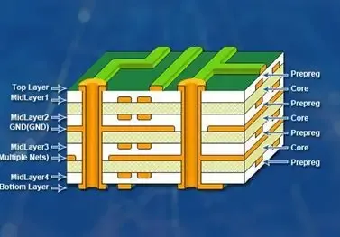
Warping originates primarily from mismatches in coefficient of thermal expansion between copper foil and the dielectric substrate during temperature excursions. When heat is applied unevenly, such as in lamination or reflow stages, the outer layers expand or contract at different rates, creating internal stresses that manifest as permanent deformation. Design asymmetries exacerbate this effect, including unequal copper distribution on opposite sides of the board or unbalanced layer stackups that fail to distribute mechanical loads evenly. Manufacturing variables, including etching patterns and plating thickness variations, further contribute by introducing localized stresses that propagate to the surface layers.
Moisture absorption in the base materials plays a significant role as well, since absorbed water expands upon heating and weakens adhesion between layers. Storage conditions prior to assembly can compound these issues if boards experience fluctuating humidity levels that allow gradual uptake. Engineers observe that boards with high resin content or certain glass weave styles show greater susceptibility when thermal profiles are aggressive. These mechanisms interact in complex ways, making root cause analysis essential for consistent production quality.
Practical Solutions and Best Practices
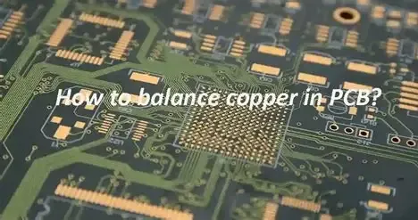
Design teams mitigate outer layer warping through symmetric copper balancing across the board, ensuring that copper percentage and distribution remain comparable on both sides. Stackup planning should prioritize symmetry in dielectric thicknesses and copper weights to minimize differential expansion forces. Material selection focuses on substrates with compatible thermal properties that reduce overall stress during processing cycles. Controlled storage in low-humidity environments prevents moisture-related expansion before boards reach the assembly line.
Process controls during fabrication include optimized lamination parameters that apply uniform pressure and temperature across the panel. Post-etch baking steps help relieve residual stresses before further handling. Inspection protocols verify flatness at multiple stages, allowing early detection and correction of deviations. These measures, when integrated into the workflow, support boards that maintain planarity through subsequent thermal exposures.
Design Guidelines for Minimizing PCB Warping
Engineers apply specific layout rules to reduce warping risk, such as distributing large copper areas evenly rather than concentrating them in isolated regions. Avoiding large solid copper pours on one side without corresponding features on the opposite side prevents torque during thermal cycling. Trace routing patterns should consider thermal mass distribution to limit localized heating effects. Documentation of stackup symmetry and copper balance percentages aids fabricators in maintaining consistency across production runs.
Collaboration between design and manufacturing teams ensures that guidelines align with actual process capabilities. Simulation tools can model thermal and mechanical behavior during the design phase, highlighting potential problem areas before fabrication begins. These proactive steps integrate seamlessly with standard qualification procedures and support higher first-pass yields.
Conclusion
Outer layer PCB warping arises from well-understood interactions among materials, design configurations, and processing conditions. Engineers who incorporate balanced layouts, appropriate material choices, and controlled handling practices achieve more consistent results. Attention to these details throughout the development cycle reduces assembly defects and enhances product reliability. Ongoing adherence to established industry practices further strengthens outcomes across diverse applications.
FAQs
Q1: What causes pcb warping in outer layers during manufacturing?
A1: Uneven copper distribution, coefficient of thermal expansion mismatches between copper and substrate, and moisture absorption represent primary contributors. Thermal stresses during lamination and reflow amplify these factors when design symmetry is lacking. Proper stackup planning and controlled storage conditions help limit the occurrence of such defects.
Q2: How does pcb bending affect assembly processes?
A2: Board distortion interferes with accurate component placement and solder joint formation, particularly for fine-pitch devices. It can also alter electrical performance in high-speed circuits by changing trace geometries and impedances. Maintaining flatness supports reliable automated assembly and reduces rework requirements.
Q3: What pcb design guidelines help prevent warping?
A3: Symmetric copper balancing across layers, even distribution of thermal mass, and selection of compatible substrate materials form core recommendations. Avoiding large asymmetric copper features and documenting stackup details for fabricators further reduce risks. These practices align with qualification expectations for rigid boards.
Q4: How should engineers address pcb manufacturing defects related to warping?
A4: Early inspection using standardized flatness measurements identifies issues before assembly. Adjustments in design symmetry and material handling, combined with process controls during fabrication, provide effective mitigation. Consistent application of these steps improves overall production stability.
References
IPC-6012E — Qualification and Performance Specification for Rigid Printed Boards. IPC, 2017
IPC-A-600K — Acceptability of Printed Boards. IPC, 2020
JEDEC J-STD-020E — Moisture/Reflow Sensitivity Classification. JEDEC, 2014


