ALLPCB


Understanding Multilayer PCBs and Layer Count
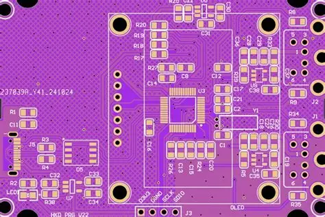
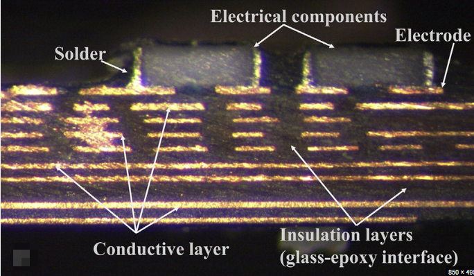
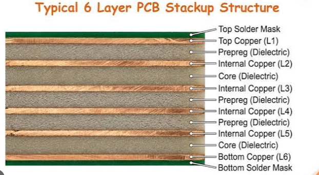
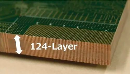
A multilayer PCB begins with a central core material that carries copper foil on both sides. Additional layers are built up using prepreg sheets and further copper foils that are laminated under heat and pressure. Two-layer boards remain common for simpler circuits, while four-, six-, and eight-layer constructions appear frequently in high-speed digital and mixed-signal designs. Each added layer increases the total number of conductive planes available for signals, power, and ground returns. PCB stackup design determines the exact sequence and thickness of every core, prepreg, and copper layer.
The choice of layer count reflects trade-offs between routing density, electromagnetic compatibility, and board rigidity. Higher layer counts allow designers to dedicate separate planes for power distribution and ground references, which reduces noise and improves return paths. Lower layer counts keep the board thinner and lighter, which benefits portable or space-constrained applications. Industry standards such as IPC-6012E guide the qualification and performance expectations for these rigid constructions across varying layer counts.
How Layer Count Influences Overall Thickness
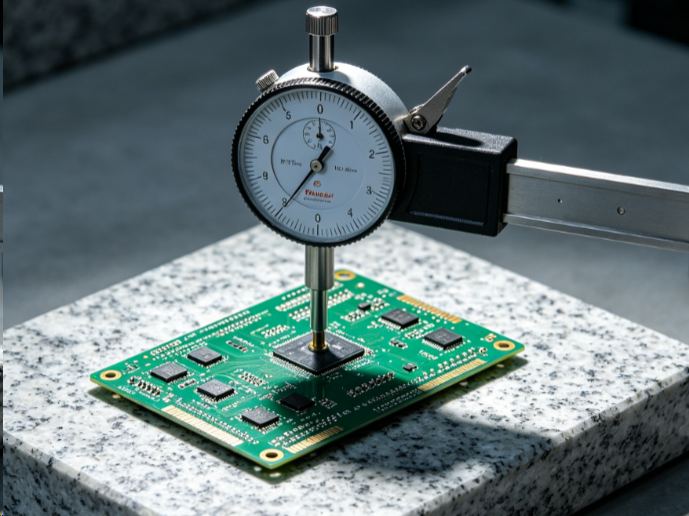
Every additional layer adds both copper thickness and dielectric material to the stackup. Copper foil typically ranges from one-half ounce to two ounces per square foot, while prepreg and core thicknesses vary according to the required dielectric spacing. As layer count rises, the cumulative height grows, although careful selection of thinner dielectrics can moderate the increase. PCB thickness calculation therefore begins with summing the individual contributions of every layer while accounting for manufacturing tolerances.
Mechanical stability improves with greater thickness because the board resists bending and vibration more effectively. Conversely, excessive thickness can create fitment issues inside enclosures or increase the distance between components and heat sinks. Designers must balance these factors during the initial stackup definition. Visual suggestions help illustrate the relationship between layer count and finished thickness.
Effects on Electrical and Thermal Performance
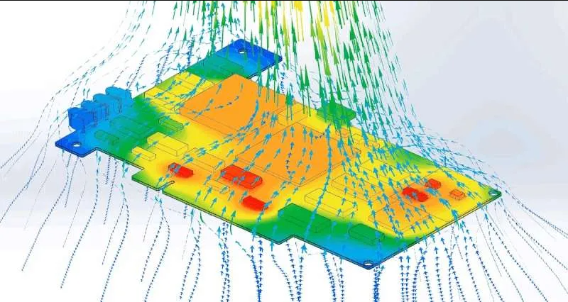
Signal integrity depends heavily on the controlled impedance achieved through precise dielectric spacing between layers. Higher layer counts provide more opportunities to route high-speed traces between dedicated reference planes, which minimizes crosstalk and electromagnetic interference. Power integrity also benefits when multiple planes distribute current and provide low-inductance paths. Thermal performance can improve because additional copper layers conduct heat away from components more effectively.
However, increased thickness lengthens the thermal path from inner layers to the board surface, potentially requiring additional thermal vias or heat-spreading techniques. Mechanical warpage risk rises with asymmetric stackups or uneven copper distribution, particularly during reflow soldering. Proper PCB stackup design addresses these issues by maintaining symmetry and balancing copper areas on opposite sides of the board.
Best Practices in PCB Stackup Design and Thickness Optimization
Engineers begin stackup planning by defining impedance targets and current-carrying requirements for each net class. They then select core and prepreg thicknesses that achieve the desired spacing while respecting the minimum dielectric requirements of IPC-A-600K. Symmetry around the central core helps control warpage, and copper balancing prevents internal stresses during lamination and thermal cycling. Software modeling of the stackup allows verification of impedance and crosstalk before fabrication.
When layer count must increase, designers evaluate whether thinner copper or high-performance laminates can offset the added height. They also consider the final assembly process, because thicker boards may require adjusted reflow profiles or specialized handling equipment. Documentation of the complete stackup, including all material types and thicknesses, ensures consistent manufacturing results across production runs.
Conclusion
Layer count directly determines the overall thickness of a multilayer PCB and shapes its electrical, thermal, and mechanical characteristics. Thoughtful PCB stackup design enables engineers to meet performance targets while controlling board height within acceptable limits. Reference to established standards such as IPC-6012E supports consistent quality across different layer configurations. By understanding these relationships, design teams can produce reliable boards that satisfy both functional and physical constraints.
FAQs
Q1: How does PCB layer count affect multilayer PCB thickness?
A1: Each additional layer adds copper foil and dielectric material, increasing the total board height. Designers calculate the cumulative thickness during stackup planning to meet both electrical and mechanical requirements. Higher layer counts generally produce thicker boards unless thinner materials are selected to compensate.
Q2: What role does PCB stackup design play in controlling thickness and performance?
A2: PCB stackup design defines the sequence, material types, and thicknesses of every layer. Proper planning achieves target impedance values, minimizes warpage, and balances copper distribution. It also ensures the finished board meets the dimensional tolerances expected by assembly processes.
Q3: Why is PCB thickness calculation important during the design phase?
A3: Accurate PCB thickness calculation prevents fitment problems in enclosures and supports reliable thermal and mechanical performance. It also allows early verification of impedance targets and helps avoid costly redesigns after fabrication. Engineers incorporate manufacturing tolerances into these calculations to maintain consistency.
Q4: How do industry standards guide multilayer PCB construction?
A4: Standards such as IPC-A-600K establish acceptability criteria for layer registration, dielectric spacing, and overall board quality. They provide measurable requirements that manufacturers and designers use to verify that finished boards meet performance expectations regardless of layer count.
References
IPC-6012E — Qualification and Performance Specification for Rigid Printed Boards. IPC, 2017
IPC-A-600K — Acceptability of Printed Boards. IPC, 2020