ALLPCB


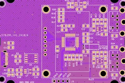
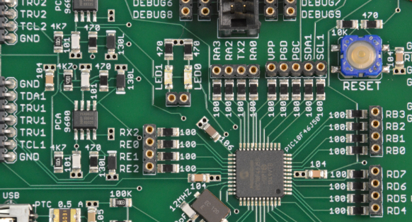
High-density interconnect designs push the limits of board real estate to support more components in smaller footprints. Silkscreen, also called the legend layer, provides essential markings for component placement, polarity indicators, and reference designators. In these compact layouts, every square millimeter counts, making the choice of font size on the silkscreen a critical design decision. Engineers must balance the need for readable text against the requirement to maintain maximum component density without introducing manufacturing defects or assembly issues. This optimization directly supports miniaturization goals while preserving the board's functionality and serviceability.
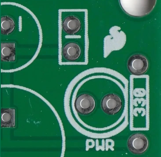
High-density PCB silkscreen refers to the ink-based legend applied to the outer layers of HDI boards to identify components and guide assembly. The layer uses epoxy or UV-curable inks printed through screens or direct imaging processes. In boards with fine-pitch components and dense routing, the silkscreen must occupy minimal space yet remain legible under typical inspection lighting. Component density silkscreen practices therefore focus on reducing character height and width while preserving contrast and adhesion. This approach enables further miniaturization PCB efforts without sacrificing the traceability required for quality control and field repairs.
What Is High-Density PCB Silkscreen and Why It Matters
The importance of small font size PCB techniques grows as devices shrink in consumer electronics, medical instruments, and automotive modules. Readable markings prevent misplacement during surface-mount assembly and simplify rework when components fail. Poor font choices can lead to ink bridging between pads or insufficient clearance from copper features, violating board acceptability criteria. Industry standards such as IPC-A-600K outline requirements for the clarity and durability of these markings on finished boards. Proper optimization therefore contributes to both higher yields and long-term reliability in high-density applications.
Technical Principles of Silkscreen in Miniaturization PCB Designs
Silkscreen application involves depositing ink onto the solder mask or bare laminate surface, where resolution depends on ink viscosity, screen mesh, and curing method. In high-density layouts, finer fonts reduce the risk of the legend overlapping traces, vias, or component pads that already sit close together. The ink must maintain sufficient line width and height to survive handling, thermal cycling, and cleaning processes without cracking or fading. Engineers evaluate font styles for stroke uniformity, favoring simple sans-serif characters that avoid thin serifs prone to breakage during printing.
Adhesion and contrast form additional constraints. The legend ink bonds to the underlying surface, and any reduction in font size must not compromise this bond or reduce visibility against the mask color. Thermal expansion differences between ink and substrate can cause delamination if the font geometry creates stress concentrations. Manufacturing tolerances in ink deposition also widen relatively as characters shrink, increasing the chance of incomplete fills or edge raggedness. These factors require designers to model the silkscreen layer alongside copper and mask features from the earliest layout stages.
Practical Solutions and Best Practices for Component Density Silkscreen
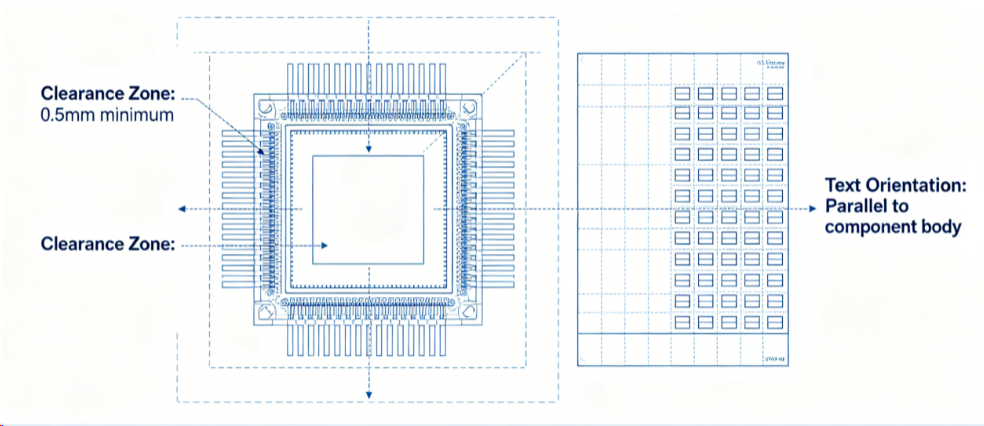
Design teams begin by selecting fonts that balance compactness with legibility at the expected viewing distance and lighting conditions. Placement algorithms in layout software can automatically adjust character size and orientation to avoid critical keep-out zones around pads and fiducials. Rotating text ninety degrees or stacking characters vertically sometimes frees horizontal space in dense areas. Clearance rules should enforce minimum distances between legend ink and exposed copper to prevent electrical shorts or mask lifting during reflow.
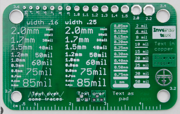
Testing the chosen font size on prototype panels verifies both print quality and functional performance. Visual inspection under magnification confirms that characters remain distinct after solder mask application and any subsequent surface finishes. Environmental stress testing, including temperature cycling and humidity exposure, checks ink durability. When issues arise, designers may increase stroke thickness slightly or switch to a different ink formulation while still targeting the smallest viable size. Collaboration between layout and fabrication teams ensures that the final silkscreen supports both assembly throughput and long-term board serviceability.
Conclusion
Optimizing silkscreen font size in high-density PCB designs requires careful attention to readability, manufacturability, and spatial efficiency. By applying structured engineering evaluation and adhering to established acceptability criteria, designers achieve greater component density without compromising assembly accuracy or board longevity. The resulting layouts support ongoing miniaturization trends while meeting the practical needs of production and maintenance teams. Consistent application of these principles across projects improves overall design quality and reduces the likelihood of costly revisions late in the development cycle.
FAQs
Q1: How does small font size PCB silkscreen affect component density in HDI boards?
A1: Reducing font size on the silkscreen layer frees space around pads and traces, allowing more components to fit within the same board area. This supports higher miniaturization PCB goals while still providing necessary identification markings. Engineers must verify that the smaller characters remain legible and durable according to industry standards such as IPC-A-600K.
Q2: What factors determine the minimum usable font size for high density PCB silkscreen?
A2: Key considerations include ink resolution limits, required clearance from copper features, contrast against the solder mask, and long-term adhesion under thermal and mechanical stress. Designers evaluate these elements together to ensure the legend meets both visual and functional requirements without interfering with assembly processes.
Q3: Why is component density silkscreen optimization important for miniaturization PCB projects?
A3: Effective optimization prevents the legend from consuming valuable real estate that could otherwise accommodate additional circuitry or smaller component packages. It also maintains traceability for quality control and repairs, which becomes more critical as boards grow denser and more complex.
Q4: How do engineers ensure small font size PCB markings remain acceptable under IPC standards?
A4: They apply design rules that maintain minimum line widths, character heights, and clearances while selecting fonts that print cleanly. Prototype builds undergo inspection per IPC-A-600K criteria to confirm that the final silkscreen meets clarity and durability expectations before volume production.
References
IPC-A-600K — Acceptability of Printed Boards. IPC, 2020
IPC-6012E — Qualification and Performance Specification for Rigid Printed Boards. IPC, 2017