 ALLPCB


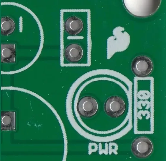
White silkscreen, also known as legend or marking ink, provides essential visual references on printed circuit boards. It indicates component positions, orientations, polarity markers, and reference designators. In PCB assembly, these markings support both automated equipment and manual processes. Clear, high-contrast silkscreen improves the speed and accuracy of component placement. This contributes directly to manufacturing optimization by reducing errors and rework.
Why White Silkscreen Matters in PCB Assembly
White silkscreen stands out against common solder mask colors such as green or blue. The high contrast helps pick and place machines locate fiducial marks and component outlines more reliably. Better visibility translates into fewer misalignments during high-speed placement cycles. Engineers and technicians also benefit when performing visual inspections or hand assembly tasks. Overall, consistent silkscreen application supports higher throughput without compromising quality.
Technical Mechanisms Supporting Silkscreen Efficiency
Silkscreen ink is applied after the solder mask and cured under controlled conditions. The white pigment reflects visible light effectively, which vision systems in pick and place machines detect with greater precision. Component alignment improves because the machine cameras can distinguish fine lines and symbols against the darker background. In contrast, lower-contrast colors may require additional lighting adjustments or slower processing speeds. Proper ink thickness and adhesion prevent flaking that could interfere with solder paste or component seating.
Industry standards such as IPC-A-600K outline acceptability criteria for legend markings to ensure they remain legible throughout assembly. When markings meet these criteria, downstream processes experience fewer interruptions. Thermal expansion differences between the ink and substrate must also stay within acceptable limits to avoid distortion during reflow.
Best Practices for Optimizing Assembly with White Silkscreen
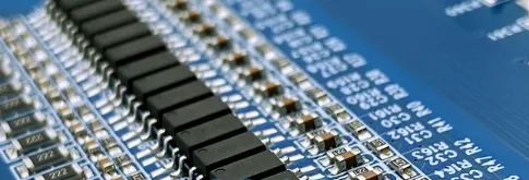
Design teams should specify silkscreen line widths and font sizes that remain readable after etching and curing. Minimum feature sizes typically follow guidelines that balance clarity with space constraints on dense boards. During manufacturing, ink application should occur uniformly to avoid thin spots or buildup near traces. Post-cure inspection verifies adhesion and contrast before panels move to assembly.
In the assembly area, operators can use the white markings as secondary references when programming placement sequences. This reduces setup time for new product introductions. Regular calibration of vision systems accounts for any slight variations in ink reflectivity across production batches. When issues arise, such as partial obscuring of markings by excess solder mask, targeted rework restores functionality without delaying the line.

Troubleshooting Common Silkscreen-Related Assembly Issues
Misaligned silkscreen can cause pick and place machines to reject components or place them incorrectly. In such cases, reviewing the artwork file against the actual board helps identify registration errors introduced during printing. Faded or low-contrast markings often result from improper curing temperatures or ink formulation mismatches. Adjusting oven profiles or switching to a higher-opacity white ink resolves visibility problems.
Another frequent issue occurs when silkscreen overlaps solder pads, which may affect paste deposition. Careful design rule checks prevent this overlap before fabrication begins. If warpage develops after reflow and distorts markings, evaluating board stack-up and support fixtures during assembly minimizes mechanical stress. Consistent application of these checks maintains silkscreen efficiency across production runs.
Conclusion
White silkscreen enhances PCB assembly efficiency through improved contrast and clear component references. It supports faster, more accurate operation of pick and place machines while aiding human operators. Attention to design specifications, application processes, and troubleshooting steps ensures these benefits are realized consistently. Manufacturers that treat silkscreen as an integral part of the assembly workflow achieve better yields and reduced cycle times.
FAQs
Q1: How does white silkscreen improve component alignment during PCB assembly?
A1: White silkscreen provides high-contrast markings that pick and place machines use to locate fiducials and component positions accurately. This reduces placement errors and supports higher production speeds without additional equipment adjustments.
Q2: What role does silkscreen efficiency play in manufacturing optimization?
A2: Efficient silkscreen application minimizes machine stoppages and rework caused by unclear markings. It allows smoother workflow from setup through final inspection, contributing to overall throughput gains in PCB assembly lines.
Q3: Can silkscreen color affect pick and place machine performance?
A3: White silkscreen offers superior reflectivity and contrast compared with darker colors, enabling vision systems to detect features more reliably. This leads to fewer alignment failures and consistent performance across varying board designs.
Q4: What standards guide acceptable silkscreen quality for assembly?
A4: Standards such as IPC-A-600K define criteria for legend legibility and adhesion that support reliable assembly processes. Following these ensures markings remain functional through soldering and handling steps.
References
IPC-A-600K — Acceptability of Printed Boards. IPC, 2020
IPC-A-610G — Acceptability of Electronic Assemblies. IPC, 2017
J-STD-001H — Requirements for Soldered Electrical and Electronic Assemblies. IPC, 2020





