 ALLPCB


Introduction
Leaded assembly remains a critical process in printed circuit board manufacturing, especially for applications requiring robust mechanical connections and high current handling. Electric engineers frequently encounter leaded assembly defects during through-hole component placement and wave or hand soldering operations. These issues can compromise electrical performance, mechanical stability, and long-term reliability if left unaddressed. Effective troubleshooting soldering techniques help identify root causes early and prevent costly rework. Understanding common problems such as solder bridges, cold solder joints, solder balls, and component misalignment supports consistent production quality.
Why Leaded Assembly Defects Matter in Modern Electronics
Leaded assembly defects directly affect the functionality of power supplies, industrial controls, and automotive modules where through-hole components provide superior strength compared to surface-mount alternatives. Solder bridges create unintended electrical shorts that can lead to immediate failures or intermittent faults under load. Cold solder joints introduce high resistance points that generate heat and degrade over time, reducing overall circuit lifespan. Component misalignment disrupts signal integrity and complicates automated testing. Addressing leaded pcb issues early in the process minimizes scrap rates and ensures compliance with performance expectations in demanding environments.
Technical Principles Behind Common Leaded Assembly Defects
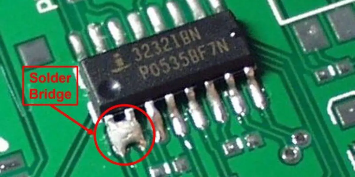
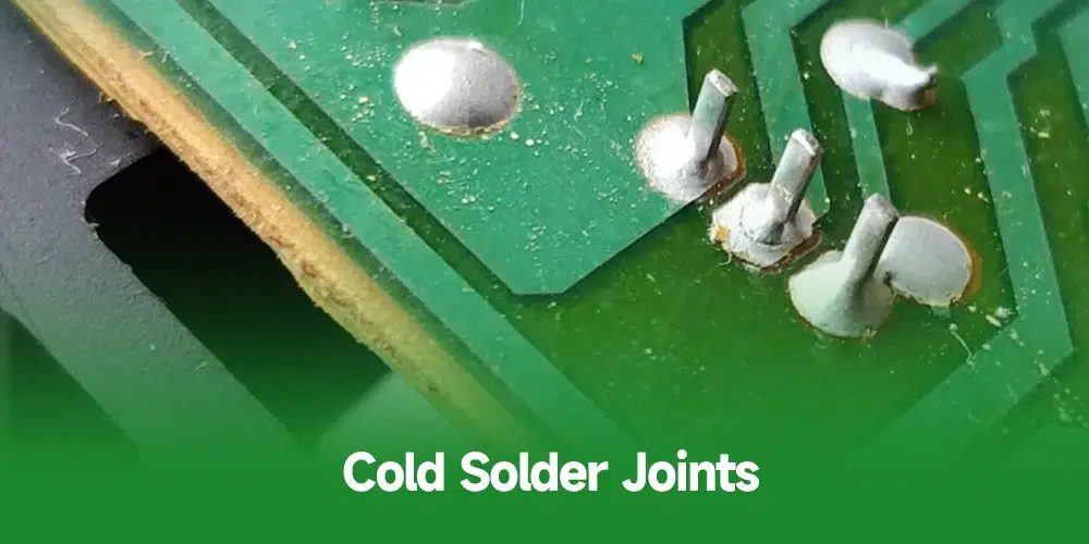
Solder bridges typically form when excess solder flows between adjacent leads due to inadequate solder mask definition or improper flux application during wave soldering. The mechanism involves surface tension and capillary action pulling molten solder into unintended areas, particularly on fine-pitch leaded packages. Cold solder joints occur when insufficient thermal energy prevents proper intermetallic compound formation between the lead, solder, and pad. This results in a dull, cracked appearance and poor electrical continuity that may pass initial testing but fail under thermal cycling. Solder balls arise from solder paste or flux residues ejecting small spheres during reflow or wave processes, often due to rapid heating rates or contaminated surfaces. Component misalignment stems from mechanical forces during insertion or uneven heating that shifts leads before solidification, violating positional tolerances required for reliable contact.
Related Reading: Bending the Rules: Component Lead Forming Techniques in Leaded Assembly
Practical Solutions and Best Practices for Troubleshooting Soldering
Begin troubleshooting by conducting visual and automated optical inspection immediately after soldering to detect solder bridges and component misalignment before further processing. Adjust wave soldering parameters such as conveyor speed, preheat temperature profiles, and solder pot levels to reduce excess solder flow and minimize bridge formation. For cold solder joints, verify thermocouple placement on the board and ensure consistent heat transfer through proper fixture design and flux activation. Implement solder ball prevention by optimizing stencil aperture design for leaded components and maintaining clean process environments to limit residue ejection. When addressing component misalignment, use precision insertion tools and verify lead forming accuracy prior to placement, followed by post-soldering X-ray verification for hidden defects. Regular process audits aligned with established industry practices help sustain defect rates below acceptable thresholds.
Related Reading: The Enduring Applications of Leaded Assembly: Where Does It Still Reign Supreme?
Troubleshooting Insights for Electric Engineers
Electric engineers benefit from a systematic approach that combines electrical testing with physical inspection to isolate leaded assembly defects quickly. Measure resistance across suspected cold solder joints using four-point probing to confirm high-resistance paths that visual checks might miss. For persistent solder balls, review the entire thermal profile and consider minor adjustments to peak temperature dwell times without exceeding component limits. When component misalignment appears repeatedly, trace the issue to feeder calibration or board fixturing rather than assuming material variation. Document each defect type with photographs and process logs to identify patterns across production batches. This practical methodology reduces downtime and supports continuous improvement in leaded pcb assembly lines.
Conclusion
Leaded assembly defects such as solder bridges, cold solder joints, solder balls, and component misalignment require targeted identification and resolution to maintain product reliability. By understanding the underlying mechanisms and applying structured troubleshooting soldering methods, engineers can achieve consistent results. Adherence to recognized standards further strengthens process control and quality outcomes. Ongoing attention to these areas supports efficient manufacturing and dependable electronic assemblies.
FAQs
Q1: What causes solder bridges in leaded assembly?
A1: Solder bridges in leaded assembly typically result from excess solder volume, inadequate solder mask clearance, or improper flux activity during wave soldering. These defects create electrical shorts between leads and can be minimized through precise process parameter control and regular equipment maintenance. Early detection via optical inspection prevents downstream failures in assembled boards.
Q2: How do cold solder joints affect leaded pcb performance?
A2: Cold solder joints in leaded pcb assemblies produce high electrical resistance and mechanical weakness because the solder fails to form a proper intermetallic bond. This leads to intermittent connections that may pass initial tests but degrade under thermal or mechanical stress. Proper preheat profiling and flux selection help eliminate these issues during troubleshooting soldering.
Q3: What steps resolve component misalignment during leaded assembly?
A3: Component misalignment during leaded assembly often stems from insertion force variations or uneven heating that shifts leads before solder solidification. Correction involves verifying lead forming accuracy, using stable fixtures, and confirming placement accuracy before soldering. Post-process inspection ensures alignment meets required tolerances for reliable operation.
Q4: How can solder balls be prevented in leaded assembly processes?
A4: Solder balls in leaded assembly arise from rapid heating or surface contamination that causes small solder particles to eject from joints. Prevention focuses on controlled thermal profiles, clean board surfaces, and optimized flux application to contain molten solder. Consistent monitoring during production reduces the occurrence of these defects.


