 ALLPCB


Industrial environments place unique demands on electronic systems. IoT devices deployed in factories, energy facilities, and outdoor installations must operate continuously amid temperature extremes, mechanical shock, vibration, dust, and moisture.
Industrial PCB design therefore focuses on selecting materials, layouts, and protective measures that maintain electrical integrity and mechanical stability over extended periods. Engineers prioritize designs that minimize failure rates while supporting the connectivity and sensing functions required by modern IoT networks.
Why Rugged PCB Design Matters in Industrial IoT
Reliable operation directly affects production uptime and safety. A single PCB failure in a process-control node can halt an entire assembly line or trigger false alarms in monitoring systems. Harsh environment PCB solutions address these risks by incorporating higher-grade substrates, reinforced mechanical features, and environmental barriers. High temperature PCB constructions, for example, use laminates with elevated glass-transition temperatures to prevent delamination during prolonged exposure above 150 degrees Celsius. Vibration resistant PCB layouts reduce stress on solder joints and component leads through strategic component placement and board stiffening. These measures collectively extend service life and lower maintenance costs in demanding applications.
Material Selection and Thermal Management Principles
Substrate choice forms the foundation of high-temperature performance. Laminates rated for continuous operation at elevated temperatures maintain dimensional stability and dielectric properties when conventional FR-4 materials would soften or degrade. Copper weight and trace geometry also influence heat dissipation; thicker copper layers spread thermal loads more effectively across the board. Component placement follows thermal modeling to keep heat-generating parts away from temperature-sensitive sensors or communication modules. Proper via stitching and thermal relief patterns further assist heat flow to heatsinks or enclosure surfaces. These engineering decisions align with established qualification methods that verify long-term reliability under thermal cycling.
Vibration and Mechanical Stress Mitigation
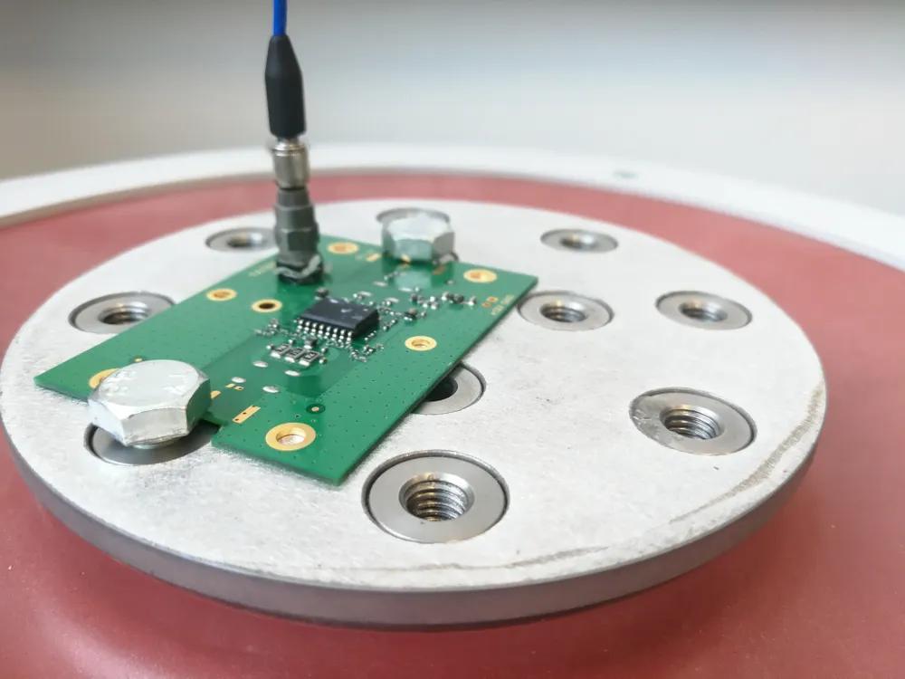
Mechanical robustness requires attention to both board-level and assembly-level factors. Mounting holes positioned at optimal locations reduce flexure during transport or equipment operation. Component selection favors parts with compliant leads or underfill where necessary. Solder joint geometry and pad design influence fatigue life under repeated vibration cycles. Board thickness and the addition of stiffeners or metal cores provide additional rigidity without excessive weight. Testing protocols evaluate resonance frequencies and acceleration levels to confirm that the assembled PCB withstands expected field conditions. Such structured approaches help ensure that industrial IoT nodes continue functioning when mounted on motors, pumps, or mobile machinery.
Protective Coatings and Environmental Barriers
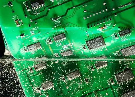
Conformal coating PCB applications supply a thin polymeric layer that shields circuitry from moisture, dust, and chemical exposure. The coating must adhere uniformly without bridging fine-pitch components or altering electrical characteristics. Selection of coating chemistry considers operating temperature range, flexibility requirements, and reworkability. Application methods such as spraying or dipping are chosen based on production volume and board complexity. Thickness verification and inspection for voids or bubbles complete the process. When combined with proper enclosure sealing, conformal coatings significantly improve long-term reliability in outdoor or wash-down environments.
Design and Assembly Best Practices
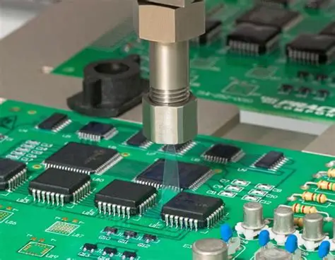
Layout practices emphasize signal integrity alongside mechanical considerations. Ground planes and power distribution networks are sized to handle both electrical loads and thermal spreading. Component orientation minimizes stress concentrations during vibration. Clearances around high-voltage or high-current areas follow spacing rules appropriate for the expected contamination levels. Documentation of stack-up, material specifications, and acceptance criteria supports consistent manufacturing outcomes. Collaboration between design and production teams helps identify potential issues before prototypes reach environmental testing.
Verification and Qualification Approach
Qualification testing follows structured sequences that replicate field stresses. Thermal cycling, humidity exposure, and mechanical shock or vibration profiles are applied according to recognized industry specifications. Visual and electrical inspections occur at defined intervals to detect early degradation. Results guide iterative improvements in layout or material choices. Documentation of test conditions and pass/fail criteria provides traceability for each production batch. This methodical process supports consistent performance across multiple deployment sites.
Conclusion
Effective industrial PCB design for IoT applications integrates material science, mechanical engineering, and environmental protection into a cohesive process. Attention to high-temperature performance, vibration resistance, and conformal coating yields assemblies that maintain functionality in challenging conditions. Adherence to established qualification standards helps engineers deliver solutions that meet both performance and longevity expectations without unnecessary complexity.
FAQs
Q1: What distinguishes industrial PCB design from standard commercial designs?
A1: Industrial PCB design incorporates higher-grade materials, reinforced mechanical features, and protective coatings to withstand temperature extremes, vibration, and contamination. These enhancements ensure reliable operation of IoT devices in factories and outdoor installations where conventional boards would fail prematurely. Engineers apply structured testing and layout practices to achieve the required durability.
Q2: How does conformal coating improve harsh environment PCB performance?
A2: Conformal coating PCB protection creates a barrier against moisture, dust, and chemicals while preserving electrical performance. The thin layer reduces corrosion risk on exposed conductors and solder joints, extending operational life in humid or dirty settings. Proper material selection and application thickness are essential for maintaining flexibility and reworkability.
Q3: What material properties support high temperature PCB operation?
A3: High temperature PCB constructions rely on substrates with elevated glass-transition temperatures that resist softening and maintain dielectric strength. Thicker copper layers and optimized thermal paths further aid heat dissipation. These characteristics allow continuous function at temperatures that would degrade standard laminates.
Q4: Why is vibration resistance critical in industrial IoT applications?
A4: Vibration resistant PCB designs prevent fatigue in solder joints and component leads caused by equipment motion or transport. Strategic component placement, board stiffening, and appropriate mounting reduce mechanical stress. This approach minimizes intermittent failures and unplanned downtime in motor-driven or mobile installations.
References
IPC-6012E — Qualification and Performance Specification for Rigid Printed Boards. IPC, 2017
IPC-A-600K — Acceptability of Printed Boards. IPC, 2020
JEDEC J-STD-020E — Moisture/Reflow Sensitivity Classification. JEDEC, 2014





