ALLPCB


Why High-Layer-Count PCBs Matter in High-Speed Digital Design
Modern high-speed digital applications transmit data at rates that make even small discontinuities significant sources of distortion. Additional layers allow designers to dedicate separate planes for power and ground, reducing noise coupling into sensitive signals. They also enable tighter control over trace geometries required for consistent impedance. Without sufficient layers, routing high-speed buses often forces compromises that degrade overall system reliability and increase the risk of electromagnetic interference.
Industry standards such as IPC-2221 guide the establishment of design rules that account for these electrical and mechanical factors in multilayer constructions. Proper layer allocation supports both signal integrity PCB goals and thermal management requirements common in high-performance equipment.
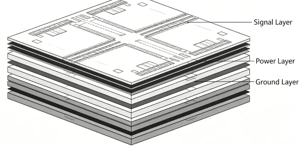
Technical Principles of Signal Integrity in Multilayer Boards
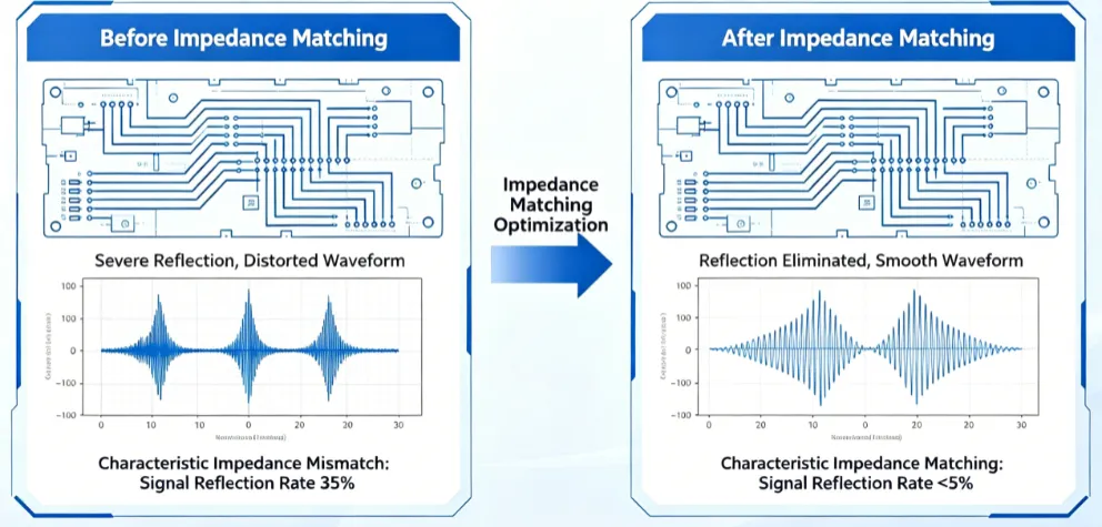
Signal integrity in high-speed digital PCB design depends on maintaining controlled impedance along every critical net. Trace width, dielectric thickness, and copper weight must be chosen together so that single-ended and differential pairs meet target impedance values, typically 50 ohms or 100 ohms. Deviations caused by layer misalignment or inconsistent dielectric constants introduce reflections that close the eye diagram at the receiver.
Power integrity also becomes more complex as layer count increases. Multiple power planes allow segmentation of voltage domains while providing low-inductance return paths for return currents. High-frequency return currents follow the path of least inductance, usually directly beneath the signal trace on an adjacent reference plane. Discontinuities such as slots in planes or poorly placed vias force currents to take longer routes, generating additional noise.
Via design requires particular attention in high-layer-count boards. Each via introduces parasitic inductance and capacitance that can affect signals above several gigahertz. Back-drilling or the use of blind and buried vias reduces stub length and improves signal quality. Material selection further influences performance; laminates with lower dissipation factor help minimize dielectric losses at higher frequencies.
Best Practices for Impedance Control and Layer Stackup
Effective impedance control PCB design begins with a well-defined stackup that balances signal layers, reference planes, and power distribution. Adjacent signal layers should reference solid planes to provide consistent return paths. Pairing high-speed signals with their reference planes on adjacent layers minimizes loop inductance and crosstalk.
Designers typically simulate proposed stackups using field solvers before committing to fabrication. These simulations account for manufacturing tolerances in dielectric thickness and trace etching. Once the stackup is finalized, layout rules enforce consistent trace widths and spacing across the board. Differential pair symmetry must be maintained, including equal length matching and avoidance of unnecessary bends.
Manufacturing considerations also influence stackup decisions. IPC-6012 specifications outline qualification requirements for rigid printed boards, including tests that verify dielectric integrity and copper adhesion in multilayer constructions. Early collaboration between design and fabrication teams helps ensure that the chosen materials and layer counts remain producible within acceptable yield limits.

Additional Considerations for High-Layer-Count Construction
Warpage control grows more challenging with increasing layer count because of differing coefficients of thermal expansion among materials. Balanced copper distribution on opposite sides of the board helps minimize bowing during thermal excursions. Sequential lamination processes may be required for very high layer counts to manage registration accuracy between layers.
Testing and validation follow fabrication. Time-domain reflectometry measurements confirm that actual impedance values match design targets across critical nets. Cross-section analysis verifies dielectric thicknesses and via fill quality. These steps close the loop between simulation predictions and physical hardware performance.
Conclusion
High-layer-count PCBs remain essential for meeting the signal integrity and routing density requirements of contemporary high-speed digital systems. Careful attention to stackup planning, impedance control, and via optimization enables reliable operation at multi-gigabit data rates. Adherence to established industry standards throughout design and manufacturing supports consistent quality and long-term reliability.
FAQs
Q1: How does layer count affect signal integrity PCB performance in high-speed designs?
A1: Higher layer counts provide dedicated reference planes and additional routing channels that help maintain consistent impedance and reduce crosstalk. Proper allocation of signal and plane layers supports cleaner return paths for high-frequency currents, preserving signal quality over longer distances and at higher data rates.
Q2: What role does impedance control PCB play when designing high-layer-count boards?
A2: Impedance control ensures that trace geometries and dielectric properties produce the target characteristic impedance for single-ended and differential signals. In high-layer-count constructions, this control must be maintained across multiple layers while accounting for manufacturing variations and the effects of vias and plane discontinuities.
Q3: Why are high-layer-count PCBs preferred for high-speed digital PCB design applications?
A3: They supply the plane resources needed for effective power distribution and electromagnetic shielding while allowing dense routing of high-speed buses without excessive layer transitions. This architecture reduces the need for compromises that would otherwise degrade timing margins or increase electromagnetic emissions.
Q4: What standards guide the design of high-layer-count PCBs for high-speed applications?
A4: Standards such as IPC-2221 and IPC-6012 provide design guidelines and qualification criteria that address electrical performance, mechanical stability, and reliability in multilayer rigid boards. Following these documents helps ensure that finished boards meet the electrical and physical requirements of demanding digital systems.
References
IPC-2221B — Generic Standard on Printed Board Design. IPC, 2012
IPC-6012E — Qualification and Performance Specification for Rigid Printed Boards. IPC, 2017