 ALLPCB


Are you looking to streamline the manufacturing process for weather station PCBs, from prototype to full-scale production? At ALLPCB, we understand the challenges of creating high-quality, cost-effective printed circuit boards (PCBs) for weather monitoring devices. In this comprehensive guide, we’ll walk you through the entire journey of weather station PCB manufacturing, focusing on key aspects like design, assembly techniques, cost optimization, and quality control. Whether you're an engineer or a business scaling up production, this post will provide actionable insights to ensure your PCBs meet performance and durability standards.
Weather stations rely on precise electronics to measure environmental factors like temperature, humidity, and pressure. The PCB is the heart of these devices, and manufacturing them efficiently requires a strategic approach. Let’s dive into the detailed steps of the weather station PCB manufacturing process, explore advanced PCB assembly techniques, and share tips for cost-effective PCB production and weather station PCB quality control.
Why Weather Station PCBs Require Special Attention
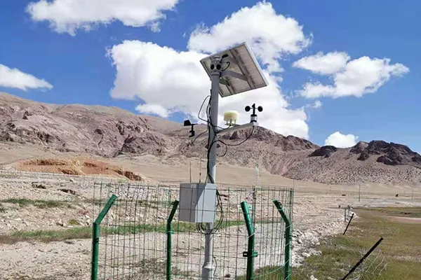
Weather stations operate in diverse and often harsh environments, from scorching deserts to freezing mountains. The PCBs inside these devices must withstand extreme temperatures, humidity, and even dust or water exposure. This makes the design and manufacturing process unique compared to standard consumer electronics. A poorly designed or manufactured PCB can lead to inaccurate readings or device failure, which is unacceptable for applications like agriculture, disaster prediction, or climate research.
At ALLPCB, we prioritize durability and precision in every step of PCB production for weather stations. From selecting robust materials to implementing strict quality checks, our goal is to ensure your weather station performs reliably under any condition.
Step 1: Designing Weather Station PCBs for Reliability
The journey from prototype to production begins with a well-thought-out design. A good design minimizes errors during manufacturing and ensures the PCB can handle the specific demands of a weather station. Here are key considerations during the design phase:
- Material Selection: Use materials like FR-4 with high thermal stability or polyimide for flexibility and heat resistance. These materials can endure temperature swings from -40°C to 85°C, common in outdoor settings.
- Component Placement: Position sensitive components like sensors away from heat-generating parts to avoid interference. For instance, a temperature sensor placed near a power regulator might give inaccurate readings due to localized heat.
- Trace Width and Spacing: Ensure trace widths support the current load, typically around 0.2-0.3mm for low-power weather station circuits, to prevent overheating. Maintain spacing of at least 0.15mm to avoid signal crosstalk, especially for high-frequency data transmission.
- Environmental Protection: Incorporate conformal coating or encapsulation in the design plan to shield the PCB from moisture and dust, extending its lifespan in outdoor conditions.
By optimizing the design early, you reduce the risk of costly revisions during prototyping or production. ALLPCB offers design review services to catch potential issues before manufacturing begins, saving you time and resources.
Step 2: Prototyping Weather Station PCBs
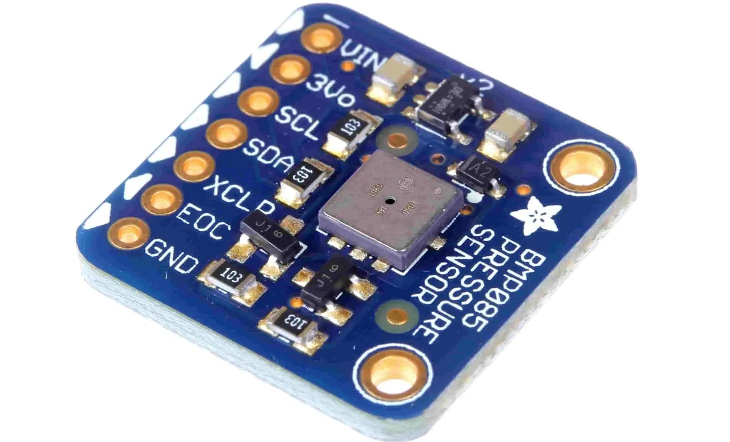
Prototyping is a critical phase in the weather station PCB manufacturing process. It allows you to test the design under real-world conditions before committing to mass production. Here’s how to streamline this stage:
- Small Batch Production: Start with a small run of 5-10 PCBs to evaluate functionality. This minimizes costs if design flaws are detected.
- Testing for Accuracy: Test the prototype in simulated environmental conditions. For example, place the weather station PCB in a chamber with 90% humidity and 50°C to verify sensor accuracy and board integrity.
- Feedback Loop: Use test data to refine the design. If a sensor fails to deliver accurate readings within a 1% error margin, adjust its placement or shielding.
ALLPCB supports rapid prototyping with quick turnaround times, ensuring you can iterate designs efficiently without delays in your project timeline.
Step 3: Mastering PCB Assembly Techniques for Weather Stations
Once the prototype is validated, it’s time to focus on production. PCB assembly techniques play a huge role in determining the quality and cost of the final product. For weather station PCBs, precision and reliability are non-negotiable. Here are the assembly methods we recommend:
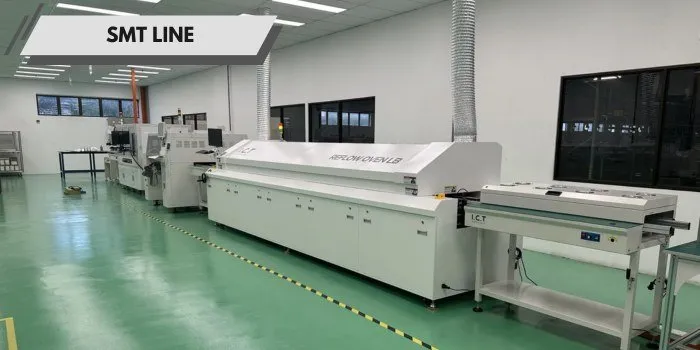
- Surface Mount Technology (SMT): Most weather station components, like microcontrollers and sensors, are surface-mounted for compactness. SMT allows for automated assembly, reducing labor costs and improving placement accuracy to within 0.01mm.
- Through-Hole Assembly: For components that need extra mechanical strength, such as connectors exposed to vibration in outdoor setups, through-hole technology provides durability. This method ensures a stronger bond but may increase assembly time.
- Mixed Assembly: Combining SMT and through-hole techniques is often ideal for weather station PCBs, balancing compactness with robustness.
- Automated Pick-and-Place: Using automated machines for component placement speeds up assembly and reduces human error, especially for small components like 0402 resistors or capacitors commonly used in compact weather station designs.
ALLPCB leverages state-of-the-art assembly equipment to ensure every component is placed with precision, minimizing defects during production runs.
Step 4: Achieving Cost-Effective PCB Production
Balancing quality and cost is a top priority for any manufacturer. Cost-effective PCB production doesn’t mean cutting corners; it means optimizing every stage of the process. Here are strategies to reduce expenses without sacrificing performance:
- Bulk Ordering: Ordering materials and components in larger quantities often lowers the per-unit cost. For example, producing 1,000 PCBs instead of 100 can reduce costs by up to 30% due to economies of scale.
- Panelization: Grouping multiple PCBs on a single panel during manufacturing reduces material waste and speeds up production. A well-designed panel can increase efficiency by fitting 10-20 small weather station PCBs in one go.
- Standardized Components: Use widely available components instead of custom parts to avoid high costs and supply chain delays. For instance, a standard temperature sensor with a 0.5°C accuracy is often sufficient for most weather stations and costs less than a niche alternative.
- Minimizing Layers: Keep the PCB design to 2-4 layers unless additional layers are necessary for complex routing. Each additional layer can increase production costs by 10-15%.
ALLPCB offers competitive pricing and flexible production options to help you achieve cost-effective PCB production while maintaining high standards for your weather station projects.
Step 5: Implementing Weather Station PCB Quality Control
Quality control is the backbone of reliable weather station PCBs. Without strict checks, even a well-designed PCB can fail in the field. Weather station PCB quality control must be rigorous to ensure every board meets performance and durability standards. Here’s how we approach it:
- Automated Optical Inspection (AOI): AOI machines scan every PCB for soldering defects, misaligned components, or missing parts. This ensures 100% inspection coverage with a defect detection rate of over 99%.
- X-Ray Testing: For hidden solder joints under components like Ball Grid Arrays (BGAs), X-ray testing verifies connection integrity, critical for high-density weather station designs.
- Functional Testing: Each PCB undergoes functional tests to simulate real-world conditions. For example, we test if the humidity sensor outputs data within a 2% accuracy range at 80% relative humidity.
- Environmental Stress Testing: Subject PCBs to extreme conditions, such as thermal cycling between -20°C and 70°C, to confirm they won’t crack or delaminate in harsh weather.
At ALLPCB, every weather station PCB passes through multiple quality control stages before shipment, giving you confidence in the reliability of your devices.
Step 6: Scaling from Prototype to Full Production
Transitioning from prototype to full production requires careful planning to avoid bottlenecks. Here’s how to scale efficiently:
- Supply Chain Management: Secure a steady supply of components to prevent delays. Lock in suppliers for critical parts like sensors to avoid shortages during high-volume runs.
- Manufacturing Capacity: Partner with a manufacturer that can handle both small prototypes and large production runs without compromising on lead times or quality.
- Documentation: Maintain detailed records of the prototype design, test results, and assembly instructions to ensure consistency as production scales up.
ALLPCB provides end-to-end support, from initial prototyping to mass production, ensuring a smooth scale-up with minimal disruptions.
Common Challenges in Weather Station PCB Manufacturing and How to Overcome Them
Manufacturing PCBs for weather stations isn’t without challenges. Here are some common issues and solutions:
- Signal Interference: Outdoor environments can introduce electromagnetic interference (EMI). Use ground planes and shielding in the design to maintain signal integrity, keeping noise levels below 50mV for critical sensor data.
- Component Failures: Harsh conditions can degrade components. Select parts with wide operating ranges (e.g., capacitors rated for -55°C to 105°C) and apply protective coatings.
- Cost Overruns: Unexpected design changes can inflate costs. Conduct thorough design reviews and prototyping tests to catch issues early.
With ALLPCB’s expertise, we help navigate these challenges by offering tailored solutions at every stage of production.
Conclusion: Partnering for Success in Weather Station PCB Manufacturing
From prototype to production, streamlining the manufacturing of weather station PCBs requires attention to detail, advanced PCB assembly techniques, and a commitment to weather station PCB quality control. By focusing on robust design, efficient assembly, and cost-effective PCB production, you can create reliable weather monitoring devices that stand up to the toughest conditions.
ALLPCB is here to support you through every step of the weather station PCB manufacturing process. With our cutting-edge facilities, rigorous quality standards, and dedication to customer satisfaction, we ensure your PCBs are built to perform. Ready to start your next weather station project? Let us help you bring your vision to life with precision and efficiency.





