 ALLPCB


Introduction
In the realm of power electronics and high-current applications, 2oz copper PCBs stand out for their ability to handle substantial thermal loads and current densities. Electrical engineers often start with PCB prototyping to validate designs, but scaling to production introduces complexities in the PCB fabrication process. Thicker copper layers demand precise control over plating, etching, and lamination to avoid defects like warpage or poor adhesion. This transition requires a deep understanding of material behaviors and process optimizations to ensure reliability at volume scales. For instance, prototype runs might tolerate minor variations, while production demands consistency aligned with industry benchmarks. Mastering 2oz copper PCB manufacturing bridges the gap between innovation and manufacturability, enabling robust products in sectors like renewable energy and electric vehicles.
What Is 2oz Copper PCB Manufacturing and Why It Matters
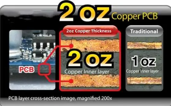
2oz copper PCB manufacturing refers to boards with copper foil weighing 2 ounces per square foot, translating to approximately 70 microns in thickness per layer. This contrasts with standard 1oz copper at 35 microns, providing enhanced current-carrying capacity and reduced resistance for high-power circuits. Engineers select 2oz copper for applications requiring efficient heat dissipation, such as motor drives, inverters, and RF amplifiers, where trace widths can be narrower without overheating. The relevance intensifies in modern designs pushing power densities, as thinner copper would necessitate wider traces, complicating layout and increasing board size. Moreover, in multilayer stacks, 2oz layers improve overall thermal performance, critical for systems operating under sustained loads. As designs evolve toward compactness, 2oz copper PCB manufacturing becomes essential for balancing electrical performance with physical constraints.
The PCB fabrication process for these boards involves specialized steps to maintain copper integrity across layers. During prototyping, small batches allow experimentation with parameters, but production scales amplify the need for uniformity. Variations in copper thickness can lead to impedance mismatches or electromigration failures over time. Thus, understanding these fundamentals equips engineers to anticipate scaling hurdles early.
Technical Principles Behind 2oz Copper PCB Fabrication
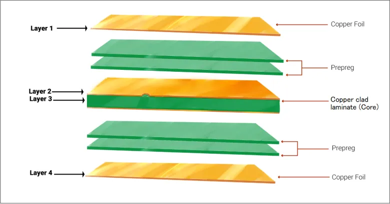
The core of 2oz copper PCB manufacturing lies in the interplay of lamination, imaging, and plating processes tailored for heavier copper weights. In the fabrication process, copper foil is laminated onto substrate cores using high-pressure presses to achieve void-free bonds, with resin flow critical to prevent delamination under thermal stress. For prototypes, single-sided or simple double-sided builds suffice, but production often involves sequential build-up for multilayers, where inner layers receive electrodeposited copper to reach 2oz thickness. Etching precision becomes paramount, as thicker copper requires deeper etchant penetration and controlled undercut to preserve trace geometries. Drilling challenges arise due to copper's ductility, potentially causing burrs or smear that demand aggressive plasma desmear cycles.
Plating uniformity represents another key mechanism, especially in through-hole plating where electrolytic copper deposition must fill vias without voids. Engineers must account for current density distribution across panels, as edge effects can thin copper peripherally. In production, panel sizes expand from prototype's 18x24 inches to full sheets, necessitating rack plating systems for consistent thickness. Adhesion testing per IPC-6012E ensures peel strength exceeds minimums, guarding against reliability issues in harsh environments. These principles underscore why 2oz copper demands process controls beyond standard boards.
Warpage control emerges as a dominant factor, driven by copper's coefficient of thermal expansion mismatch with FR-4 substrates. Thicker copper exacerbates bowing during lamination cooldown, potentially misaligning layers. Fabrication facilities mitigate this through symmetric stack-ups and constrained pressing.
The PCB Prototyping Process for 2oz Copper Boards
PCB prototyping for 2oz copper begins with material selection, favoring high-Tg laminates to withstand plating chemistries and thermal cycles. Dry film photoresist imaging defines traces, followed by spray etching to remove excess copper selectively. Engineers often iterate designs here, adjusting trace widths via simulation to meet current ratings without excessive heat rise. Vias are mechanically drilled and plated with electroless copper seed layers before electrolytic buildup to full thickness. Quick-turn prototypes use smaller panels to minimize setup times, allowing same-day deliveries for validation.
Post-etch inspection verifies line widths and spacing, with optical comparators spotting defects early. Solder mask application protects traces, cured under UV for durability. Electrical testing confirms continuity and shorts absence before shipping. This agile PCB prototyping phase uncovers design flaws cost-effectively, but tolerances are looser than production.
Challenges include higher etching times, risking over-etch if not monitored, and plating cracks from hydrogen embrittlement. Prototype fabs compensate with pulse plating to enhance ductility.
Scaling to Production: Key Changes in the PCB Fabrication Process
Transitioning 2oz copper PCB manufacturing to production shifts from artisanal prototyping to automated, high-volume flows. Larger panel formats, like 18x24 inches or bigger, enable economies of scale, but demand fly-back etching lines for uniform copper removal across expansive areas. Multilayer production employs X-ray registration for inner layer alignment, crucial as 2oz copper amplifies misalignment impacts on via reliability. Outer layer imaging uses laser direct imaging for finer features, followed by tin plating to protect against oxidation.
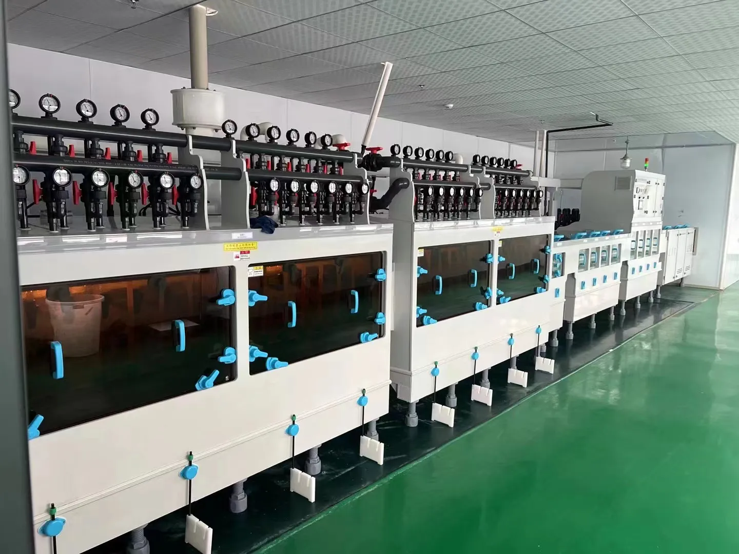
Through-hole plating scales via vertical continuous plating lines, depositing copper at rates ensuring 25-micron minimum buildup. Desmear and activation steps intensify to handle debris from thicker drills. Final profiling uses routing or scoring for depanelization, with tabs preventing tab-out distortions.
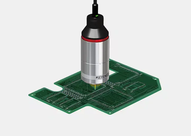
Quality control escalates per IPC-A-600K criteria, incorporating automated optical inspection for trace defects and cross-sectioning for plating thickness verification. Solderability preservation involves hot air solder leveling or ENIG finishes suited to heavy copper.
Production routing introduces stress relief slots to combat warpage, tested via shadow moire methods.
PCB Assembly Considerations for Scaled 2oz Copper Boards
Once fabricated, PCB assembly for 2oz copper demands adaptations in soldering and component placement. Thicker copper alters reflow profiles, with higher thermal mass slowing heat-up and risking cold joints on fine-pitch parts. Solder paste volume increases for vias to ensure fill, per J-STD-001 requirements for joint integrity. Selective soldering suits through-hole components, avoiding blanket wave exposure that warps boards.
Stencil design incorporates thicker foils for adequate paste release on wide traces. Post-reflow x-ray inspects BGA voids, critical as 2oz planes influence underfill flow. Thermal profiling ensures peak temperatures align with component limits, preventing copper dissolution into solder.
Assembly yields improve with fixtureless handling via edge support, minimizing bow-induced misregistration.
Best Practices for Successful Scaling
Engineers should prioritize design for manufacturability from prototyping onward. Minimum trace widths for 2oz copper typically exceed 0.15mm to accommodate etching tolerances, with annular rings sized for plating throw. Panelization uses 3-2-3 V-scoring for efficient depanelization, reducing stress concentrations.
Material choices include low-CTE cores to match copper expansion, minimizing warpage below 0.75% per IPC standards. Fabrication partners communicate aspect ratios under 10:1 for vias to avoid plating voids. Incoming inspections verify copper weight via beta backscatter.
Troubleshooting common issues like delamination involves bake-out cycles pre-lamination to remove moisture. For warpage, counterbalance copper placement symmetrically.
Production qualification runs validate process capability, tracking CpK values above 1.33 for critical features.
Conclusion
Scaling 2oz copper PCB manufacturing from prototype to production transforms engineering concepts into reliable, high-volume products. Key lies in mastering fabrication nuances like plating uniformity and warpage control, alongside assembly adaptations for thermal realities. Adhering to standards ensures consistency, while best practices streamline the transition. Electrical engineers benefit from this structured approach, delivering performant boards for demanding applications. Ultimately, proactive design and process awareness minimize risks, fostering efficient PCB prototyping to production pipelines.
FAQs
Q1: What are the main challenges in the PCB fabrication process for 2oz copper PCB manufacturing?
A1: Thicker copper increases etching times and warpage risks due to CTE mismatch with substrates. Plating uniformity across large panels requires precise current control to avoid thin spots. Fabrication facilities address these via pulse plating and symmetric stack-ups, aligning with IPC-6012E for performance specs. Prototype tolerances loosen, but production demands tighter controls for yield.
Q2: How does PCB prototyping differ from full-scale 2oz copper PCB manufacturing?
A2: Prototyping uses small panels and manual steps for quick iterations, tolerating minor variations. Production scales to large sheets with automated lines for cost efficiency in the PCB fabrication process. Engineers focus on DFM in prototypes to ease scaling, ensuring via fills and trace integrity transfer seamlessly.
Q3: What role does quality control play in scaling PCB assembly for 2oz copper boards?
A3: Quality control per IPC-A-600K verifies plating thickness and solderability post-fabrication. In assembly, x-ray and thermal profiling detect voids exacerbated by copper's thermal mass. This prevents field failures, maintaining J-STD-001 compliance for joint reliability in high-current apps.
Q4: Why is panelization critical in 2oz copper PCB manufacturing production?
A4: Panelization optimizes material use and handling in automated lines, with scoring preventing warpage during depanelization. It ensures uniform processing across arrays, vital for consistent 2oz copper deposition. Poor panel design leads to edge effects, impacting yield in the PCB fabrication process.
References
IPC-6012E — Qualification and Performance Specification for Rigid Printed Boards. IPC, 2017
IPC-A-600K — Acceptability of Printed Boards. IPC, 2020
J-STD-001G — Requirements for Soldered Electrical and Electronic Assemblies. IPC, 2011





