 ALLPCB


Introduction
Flex PCBs play a vital role in modern electronics, enabling compact designs in wearables, medical devices, and high-speed interconnects. As signal speeds increase, maintaining precise impedance becomes essential to prevent signal degradation, reflections, and data errors. PCB thickness directly influences this impedance, particularly the dielectric layers that separate conductors from reference planes. Engineers must balance flexibility requirements with electrical performance during design. This article explores flex PCB impedance, the impact of thickness variations, and strategies for effective control. Understanding these relationships ensures reliable operation in demanding applications.
Understanding Flex PCB Impedance and Its Importance
Characteristic impedance in flex PCBs refers to the opposition to alternating current flow along transmission lines, determined by geometry and material properties. In high-frequency signals, mismatches cause reflections that distort waveforms and reduce signal integrity. Flex PCB impedance control is crucial for applications like USB, HDMI, and RF modules where tolerances of 10 percent or tighter are common. Without proper control, issues such as crosstalk, attenuation, and timing skew arise. Industry standards like IPC-2223 provide guidelines for designing transmission lines in flexible circuits. Prioritizing impedance from the outset minimizes costly redesigns and iterations.
Thinner flex constructions enhance bendability but complicate impedance matching due to reduced dielectric spacing. Engineers target single-ended impedances around 50 ohms or differential pairs at 100 ohms, adjusting parameters accordingly. Flex materials like polyimide offer stable dielectric constants, aiding predictability. However, manufacturing tolerances in thickness can shift values by several ohms if not managed. Proactive design verifies performance through simulation and test coupons. This foundation supports robust, high-yield production.
How PCB Thickness Affects Impedance in Flexible Circuits
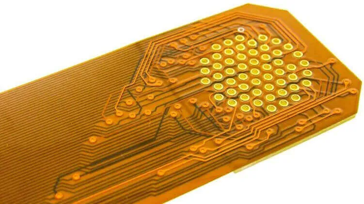
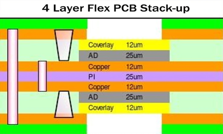
Dielectric thickness is the dominant factor in determining characteristic impedance, as it sets the distance between signal traces and ground planes. Increasing dielectric height raises impedance by reducing capacitive coupling, while thinner layers lower it by bringing conductors closer. In flex PCBs, the base dielectric and coverlay contribute to total thickness, often ranging from 25 to 125 micrometers combined. Copper trace thickness also plays a role, though secondary, as thicker metal reduces inductance slightly. Variations during lamination or etching can alter effective height, impacting final values.
Polyimide films exhibit dielectric constants around 3.2 to 3.5, lower than FR-4, which allows wider traces for the same impedance compared to rigid boards. PCB thickness and impedance relationships follow transmission line theory, where impedance scales inversely with the square root of dielectric height for microstrip lines. Flex circuits often use microstrip or stripline configurations, with striplines offering better shielding but requiring symmetric thicknesses. Bending introduces minor shifts, typically under 5 percent if bend radius exceeds 10 times the circuit thickness. Factory processes must maintain tight tolerances to preserve design intent. Consistent thickness control aligns with qualification specs in IPC-6013.
Manufacturing dielectric layers involves precise adhesive and film bonding, where inconsistencies lead to impedance spreads. Engineers specify minimum coverlay thicknesses to avoid over-etching traces during processing. Test structures on panels verify actual values post-fabrication. These practices ensure flex PCB impedance remains within spec across production lots.
Key Factors Influencing Impedance Control in Flexible Circuits
Beyond thickness, trace width and spacing define the inductive and capacitive balance for target impedance. Wider traces lower impedance by increasing capacitance, while narrower ones raise it. Reference plane design, often hatched in flex to maintain flexibility, affects field distribution and shielding effectiveness. Material anisotropy in polyimide under stress from flexing can cause slight directional variations in dielectric constant. Humidity and temperature further modulate values, with polyimide showing good stability up to 150 degrees Celsius.
Stackup configuration dictates whether microstrip, embedded microstrip, or stripline is feasible. Single-layer flex favors coplanar waveguide for ground proximity without added layers. Multilayer rigid-flex transitions demand matched impedances across sections. Copper weight, typically 1/2 or 1 oz, influences skin effect at gigahertz frequencies. All parameters interact, requiring iterative field solver analysis.
Adhesiveless laminates improve thickness uniformity over bonded types, reducing voids that trap air and alter effective dielectric constant. Ground plane patterning, like cross-hatching, preserves bend radius while supporting impedance. These choices optimize both mechanical and electrical performance.
Best Practices for Impedance Control Through Thickness Management
Start with accurate stackup modeling using field solvers that account for flex-specific materials and geometries. Specify dielectric thicknesses with tolerances like plus or minus 10 percent, tighter for high-speed designs. Collaborate with fabricators early to confirm process capabilities for thin cores. Include impedance test coupons on production panels, measuring time-domain reflectometry post-fabrication.
Layer sequencing minimizes thickness buildup in bend areas, using tapered transitions where possible. For striplines, ensure symmetric dielectrics above and below traces to avoid mode conversion. Coverlay application demands uniform lamination pressure to prevent bubbles. Post-etch inspection verifies trace profiles.
IPC-4101 specifications guide base material selection for consistent dielectric properties. Verification involves vector network analyzers for S-parameters, confirming return loss below minus 10 dB. These steps yield predictable flex PCB impedance across volumes.
Challenges in Flex PCB Design and Troubleshooting Solutions
Material variations pose the primary hurdle, as polyimide thickness control lags rigid epoxy due to film handling. Bending cycles induce microcracks or delamination, shifting impedance over time. Transitions to rigid sections create stubs that radiate noise if unmatched.
Mitigate with design rules: bend radii at least six times thickness for static flex, ten times for dynamic. Use shielding layers judiciously to avoid stiffness. Simulate bending effects via finite element models integrated with EM solvers.
Fabrication challenges include etch factor in thin coppers, leading to trapezoidal profiles that raise impedance. Compensate by widening design widths. Qualification testing per IPC standards confirms reliability under flex cycles.
Conclusion
Flex PCB thickness profoundly impacts impedance, dictating signal integrity in compact, dynamic applications. Engineers achieve control by mastering dielectric spacing, trace geometry, and material choices. Adhering to standards like IPC-2223 and IPC-6013 ensures manufacturability and performance. Proactive simulation, tight tolerances, and verification form the backbone of success. Balancing flexibility with electrical demands yields innovative, reliable designs. Prioritizing these considerations elevates project outcomes.
FAQs
Q1: What role does dielectric thickness play in flex PCB impedance?
A1: Dielectric thickness primarily governs capacitive coupling between traces and grounds, directly affecting characteristic impedance. Thinner layers decrease impedance by proximity, while thicker ones increase it. In flexible circuits, base films and coverlays must maintain uniformity to hit targets like 50 ohms single-ended. Factory processes align with IPC-6013 tolerances for consistency.
Q2: How can engineers optimize PCB thickness and impedance in design?
A2: Use stackup calculators and EM simulators to iterate trace width against dielectric height for desired impedance control in flexible circuits. Specify polyimide with stable Dk and request fabricator DFM reviews. Include TDR coupons for validation. Avoid overly thin constructions that compromise yield.
Q3: Does bending affect impedance control in flex PCBs?
A3: Minimal shifts occur if bend radius exceeds 10 times thickness, keeping changes under 5 percent. Hatched grounds preserve flexibility without degrading shielding. Test under operational cycles to confirm stability. Standards guide minimum radii for reliability.
Q4: What are common tolerances for flex PCB impedance?
A4: Typical single-ended control aims for plus or minus 10 percent, tighter for differential pairs. Thickness variations drive spreads, so select processes with precise lamination. Post-fab measurement ensures compliance before assembly.





