 ALLPCB


What Is Fanout Design and Why It Matters
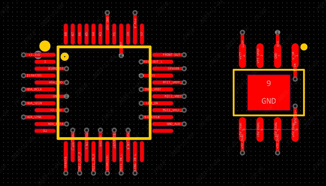
Fanout design describes the systematic routing of traces from component pads to vias or other interconnect points so that signals can reach inner layers or distant board areas. In practice, designers select via types, stack-up configurations, and escape paths that respect minimum feature sizes dictated by the fabrication process. The approach becomes critical because modern components pack hundreds of connections into small footprints, leaving limited real estate for routing without violating clearance rules. Poor fanout choices can increase the risk of open circuits during etching or create solder bridges during reflow. Attention to fanout design solderability ensures pads remain accessible for proper wetting while fanout design testability maintains probe access for in-circuit or boundary-scan verification. Overall, optimized fanout contributes to higher first-pass yield and lower rework rates throughout the manufacturing flow.
Technical Principles of Fanout Design
The core engineering challenge in fanout lies in balancing trace width, via diameter, and annular ring dimensions against the tolerances of the fabrication process. Designers typically begin by mapping the component footprint and identifying the most direct escape routes that avoid layer-to-layer via stacking conflicts. Differential pair routing within fanout regions requires matched lengths and controlled impedance, which adds constraints on via placement and trace geometry. Thermal relief connections around power vias help manage heat during soldering yet must not compromise current-carrying capacity. When these principles are applied consistently, the resulting layout supports both high-speed signal integrity and mechanical robustness under thermal cycling. Industry standards such as IPC-6012E provide qualification criteria for rigid boards that encompass via and trace features arising from fanout decisions.
Practical Solutions and Best Practices
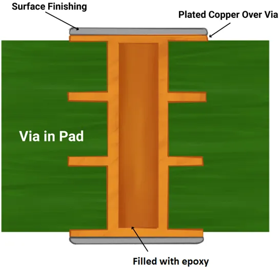
Engineers improve fanout design assembly outcomes by selecting via-in-pad or microvia technologies only when board thickness and aspect ratios permit reliable plating. Placing test points on outer layers during fanout layout enhances fanout design testability without adding extra vias that could affect routing density. Maintaining consistent copper distribution across the board helps control warpage during lamination and reflow, which in turn protects solder joint integrity. Designers also review drill-to-copper clearances and solder mask expansion rules early to prevent mask encroachment on pads. When these practices are followed, the layout remains compatible with standard fabrication and assembly equipment while meeting reliability targets. Reference to IPC-A-600K acceptance criteria guides visual and dimensional inspection of features created by fanout routing.
Ensuring Reliability and Yield Through Integrated Considerations
Reliability in fanout regions depends on managing stress concentrations at via-to-pad transitions and ensuring adequate solder volume for each joint. Thermal expansion mismatch between the component package and the board can be mitigated by symmetric fanout patterns that distribute mechanical load evenly. Yield improvements often result from iterative design reviews that simulate fabrication tolerances before release to manufacturing. Incorporating fanout design fabrication rules such as minimum annular ring size and via fill requirements reduces the incidence of plating voids or etch undercut. These measures collectively support consistent electrical performance and mechanical durability over the product lifecycle.
Conclusion
Thoughtful fanout design integrates manufacturability, solderability, testability, assembly, and fabrication requirements from the earliest layout stages. By applying structured engineering principles and referencing established industry standards, designers achieve higher yields and more reliable boards without unnecessary complexity. The result is a manufacturing process that consistently delivers functional products meeting performance expectations.
FAQs
Q1: How does fanout design manufacturability affect overall PCB yield?
A1: Fanout design manufacturability influences yield by determining whether trace and via features can be produced within fabrication tolerances. Proper spacing and via selection reduce defects such as opens or shorts, allowing higher percentages of boards to pass initial electrical testing.
Q2: What role does fanout design solderability play in assembly success?
A2: Fanout design solderability ensures pads and vias accept solder consistently during reflow. Adequate mask clearance and surface finish compatibility promote reliable wetting and minimize defects such as insufficient solder or bridges.
Q3: Why is fanout design testability important for production boards?
A3: Fanout design testability provides accessible points for automated test equipment. Strategic placement of vias and test pads during routing supports thorough in-circuit or functional testing without requiring additional board area or layers.
Q4: How can engineers optimize fanout design fabrication for fine-pitch components?
A4: Engineers optimize fanout design fabrication by selecting appropriate via technologies and verifying clearances against process capabilities. Early collaboration on stack-up and feature sizes helps maintain acceptable yields even with dense interconnect patterns.


